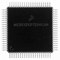
MC9S12XDT256CAA Freescale Semiconductor, MC9S12XDT256CAA Datasheet - Page 1238

MC9S12XDT256CAA
Manufacturer Part Number
MC9S12XDT256CAA
Description
IC MCU 256K FLASH 80-QFP
Manufacturer
Freescale Semiconductor
Series
HCS12r
Datasheet
1.MC9S12XD64CAA.pdf
(1348 pages)
Specifications of MC9S12XDT256CAA
Core Processor
HCS12X
Core Size
16-Bit
Speed
80MHz
Connectivity
CAN, EBI/EMI, I²C, IrDA, LIN, SCI, SPI
Peripherals
LVD, POR, PWM, WDT
Number Of I /o
59
Program Memory Size
256KB (256K x 8)
Program Memory Type
FLASH
Eeprom Size
4K x 8
Ram Size
16K x 8
Voltage - Supply (vcc/vdd)
2.35 V ~ 5.5 V
Data Converters
A/D 8x10b
Oscillator Type
External
Operating Temperature
-40°C ~ 85°C
Package / Case
80-QFP
Processor Series
S12XD
Core
HCS12
Data Bus Width
16 bit
Data Ram Size
16 KB
Interface Type
CAN/I2C/SCI/SPI
Maximum Clock Frequency
40 MHz
Number Of Programmable I/os
59
Number Of Timers
12
Maximum Operating Temperature
+ 85 C
Mounting Style
SMD/SMT
3rd Party Development Tools
EWHCS12
Development Tools By Supplier
EVB9S12XDP512E
Minimum Operating Temperature
- 40 C
On-chip Adc
8-ch x 10-bit
Lead Free Status / RoHS Status
Lead free / RoHS Compliant
Available stocks
Company
Part Number
Manufacturer
Quantity
Price
Company:
Part Number:
MC9S12XDT256CAA
Manufacturer:
Freescale Semiconductor
Quantity:
10 000
Company:
Part Number:
MC9S12XDT256CAAR
Manufacturer:
Freescale Semiconductor
Quantity:
10 000
- Current page: 1238 of 1348
- Download datasheet (8Mb)
Appendix A Electrical Characteristics
A.1.3
There are four groups of functional pins.
A.1.3.1
Those I/O pins have a nominal level in the range of 3.15 V to 5.5 V. This class of pins is comprised of all
port I/O pins, the analog inputs, BKGD and the RESET pins.The internal structure of all those pins is
identical; however, some of the functionality may be disabled. For example, for the analog inputs the
output drivers, pull-up and pull-down resistors are disabled permanently.
A.1.3.2
This group is made up by the V
A.1.3.3
The pins XFC, EXTAL, XTAL dedicated to the oscillator have a nominal 2.5 V level. They are supplied
by V
A.1.3.4
This pin is used for production testing only.
A.1.3.5
This pin is used to enable the on-chip voltage regulator.
A.1.4
Power supply must maintain regulation within operating V
operating maximum current conditions. If positive injection current (V
the injection current may flow out of V
regulation. Ensure external V
will be the greatest risk when the MCU is not consuming power; e.g., if no system clock is present, or if
clock rate is very low which would reduce overall power consumption.
1240
DDPLL
.
Pins
Current Injection
I/O Pins
Analog Reference
Oscillator
TEST
VREGEN
In the following context V
V
I
V
V
V
I
DD35
DD
SS35
DDR
DD
SSPLL
is used for the sum of the currents flowing into V
is used for V
denotes the sum of the currents flowing into the V
is used for either V
pins.
.
DD35
RH
DD1
load will shunt current greater than maximum injection current. This
and V
MC9S12XDP512 Data Sheet, Rev. 2.21
, V
DD35
DD2
SSA
RL
DD35
pins.
, V
and V
and could result in external power supply going out of
is used for either V
SSR
NOTE
DDPLL
and V
, V
SSX
DD35
SS
unless otherwise noted.
is used for V
or V
DDA
DD1
DD
, V
in
DDA
range during instantaneous and
> V
and V
DDR
, V
SS1
DD35
, and V
DDX
DD2
, V
) is greater than I
SS2
.
and
Freescale Semiconductor
DDX
and
;
DD35
,
Related parts for MC9S12XDT256CAA
Image
Part Number
Description
Manufacturer
Datasheet
Request
R

Part Number:
Description:
16-BIT MICROPROCESSOR FAMILY
Manufacturer:
FREESCALE [Freescale Semiconductor, Inc]
Datasheet:
Part Number:
Description:
Manufacturer:
Freescale Semiconductor, Inc
Datasheet:
Part Number:
Description:
Manufacturer:
Freescale Semiconductor, Inc
Datasheet:
Part Number:
Description:
Manufacturer:
Freescale Semiconductor, Inc
Datasheet:
Part Number:
Description:
Manufacturer:
Freescale Semiconductor, Inc
Datasheet:
Part Number:
Description:
Manufacturer:
Freescale Semiconductor, Inc
Datasheet:
Part Number:
Description:
Manufacturer:
Freescale Semiconductor, Inc
Datasheet:
Part Number:
Description:
Manufacturer:
Freescale Semiconductor, Inc
Datasheet:
Part Number:
Description:
Manufacturer:
Freescale Semiconductor, Inc
Datasheet:
Part Number:
Description:
Manufacturer:
Freescale Semiconductor, Inc
Datasheet:
Part Number:
Description:
Manufacturer:
Freescale Semiconductor, Inc
Datasheet:
Part Number:
Description:
Manufacturer:
Freescale Semiconductor, Inc
Datasheet:
Part Number:
Description:
Manufacturer:
Freescale Semiconductor, Inc
Datasheet:
Part Number:
Description:
Manufacturer:
Freescale Semiconductor, Inc
Datasheet:
Part Number:
Description:
Manufacturer:
Freescale Semiconductor, Inc
Datasheet:


