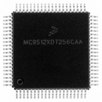
MC9S12XDT256CAA Freescale Semiconductor, MC9S12XDT256CAA Datasheet - Page 1241

MC9S12XDT256CAA
Manufacturer Part Number
MC9S12XDT256CAA
Description
IC MCU 256K FLASH 80-QFP
Manufacturer
Freescale Semiconductor
Series
HCS12r
Datasheet
1.MC9S12XD64CAA.pdf
(1348 pages)
Specifications of MC9S12XDT256CAA
Core Processor
HCS12X
Core Size
16-Bit
Speed
80MHz
Connectivity
CAN, EBI/EMI, I²C, IrDA, LIN, SCI, SPI
Peripherals
LVD, POR, PWM, WDT
Number Of I /o
59
Program Memory Size
256KB (256K x 8)
Program Memory Type
FLASH
Eeprom Size
4K x 8
Ram Size
16K x 8
Voltage - Supply (vcc/vdd)
2.35 V ~ 5.5 V
Data Converters
A/D 8x10b
Oscillator Type
External
Operating Temperature
-40°C ~ 85°C
Package / Case
80-QFP
Processor Series
S12XD
Core
HCS12
Data Bus Width
16 bit
Data Ram Size
16 KB
Interface Type
CAN/I2C/SCI/SPI
Maximum Clock Frequency
40 MHz
Number Of Programmable I/os
59
Number Of Timers
12
Maximum Operating Temperature
+ 85 C
Mounting Style
SMD/SMT
3rd Party Development Tools
EWHCS12
Development Tools By Supplier
EVB9S12XDP512E
Minimum Operating Temperature
- 40 C
On-chip Adc
8-ch x 10-bit
Lead Free Status / RoHS Status
Lead free / RoHS Compliant
Available stocks
Company
Part Number
Manufacturer
Quantity
Price
Company:
Part Number:
MC9S12XDT256CAA
Manufacturer:
Freescale Semiconductor
Quantity:
10 000
Company:
Part Number:
MC9S12XDT256CAAR
Manufacturer:
Freescale Semiconductor
Quantity:
10 000
- Current page: 1241 of 1348
- Download datasheet (8Mb)
A.1.7
This section describes the operating conditions of the device. Unless otherwise noted those conditions
apply to all the following data.
1
2
Freescale Semiconductor
I/O, regulator and analog supply voltage
Digital logic supply voltage
PLL supply voltage
Voltage difference V
Voltage difference V
Oscillator
Bus frequency
C parts
V parts
M parts
The device contains an internal voltage regulator to generate the logic and PLL supply out of the I/O supply. The absolute
maximum ratings apply when this regulator is disabled and the device is powered from an external source.
Please refer to
ambient temperature T
Operating junction temperature range
Operating ambient temperature range
Operating junction temperature range
Operating ambient temperature range
Operating junction temperature range
Operating ambient temperature range
Operating Conditions
Section A.1.8, “Power Dissipation and Thermal Characteristics”
Please refer to the temperature rating of the device (C, V, M) with regards to
the ambient temperature T
dissipation calculations refer to
Thermal
2
DDX
SSX
to V
A
to V
and device junction temperature T
1
Rating
Characteristics”.
SSR
DDR
and V
and V
SSA
DDA
2
2
2
MC9S12XDP512 Data Sheet, Rev. 2.21
Table A-4. Operating Conditions
A
and the junction temperature T
Section A.1.8, “Power Dissipation and
NOTE
J
.
Symbol
V
V
V
DDPLL
VDDX
VSSX
f
f
DD35
T J
T A
T J
T A
T J
T A
osc
bus
DD
3.15
2.35
2.35
–0.1
–0.1
for more details about the relation between
Min
–40
–40
–40
–40
–40
–40
0.5
0.5
J
. For power
Appendix A Electrical Characteristics
Typ
2.5
2.5
27
27
27
—
—
—
—
—
5
0
0
Max
2.75
2.75
100
120
105
140
125
5.5
0.1
0.1
16
40
85
MHz
MHz
Unit
V
V
V
V
V
1243
C
C
C
Related parts for MC9S12XDT256CAA
Image
Part Number
Description
Manufacturer
Datasheet
Request
R

Part Number:
Description:
16-BIT MICROPROCESSOR FAMILY
Manufacturer:
FREESCALE [Freescale Semiconductor, Inc]
Datasheet:
Part Number:
Description:
Manufacturer:
Freescale Semiconductor, Inc
Datasheet:
Part Number:
Description:
Manufacturer:
Freescale Semiconductor, Inc
Datasheet:
Part Number:
Description:
Manufacturer:
Freescale Semiconductor, Inc
Datasheet:
Part Number:
Description:
Manufacturer:
Freescale Semiconductor, Inc
Datasheet:
Part Number:
Description:
Manufacturer:
Freescale Semiconductor, Inc
Datasheet:
Part Number:
Description:
Manufacturer:
Freescale Semiconductor, Inc
Datasheet:
Part Number:
Description:
Manufacturer:
Freescale Semiconductor, Inc
Datasheet:
Part Number:
Description:
Manufacturer:
Freescale Semiconductor, Inc
Datasheet:
Part Number:
Description:
Manufacturer:
Freescale Semiconductor, Inc
Datasheet:
Part Number:
Description:
Manufacturer:
Freescale Semiconductor, Inc
Datasheet:
Part Number:
Description:
Manufacturer:
Freescale Semiconductor, Inc
Datasheet:
Part Number:
Description:
Manufacturer:
Freescale Semiconductor, Inc
Datasheet:
Part Number:
Description:
Manufacturer:
Freescale Semiconductor, Inc
Datasheet:
Part Number:
Description:
Manufacturer:
Freescale Semiconductor, Inc
Datasheet:


