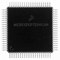
MC9S12XDT256CAA Freescale Semiconductor, MC9S12XDT256CAA Datasheet - Page 154

MC9S12XDT256CAA
Manufacturer Part Number
MC9S12XDT256CAA
Description
IC MCU 256K FLASH 80-QFP
Manufacturer
Freescale Semiconductor
Series
HCS12r
Datasheet
1.MC9S12XD64CAA.pdf
(1348 pages)
Specifications of MC9S12XDT256CAA
Core Processor
HCS12X
Core Size
16-Bit
Speed
80MHz
Connectivity
CAN, EBI/EMI, I²C, IrDA, LIN, SCI, SPI
Peripherals
LVD, POR, PWM, WDT
Number Of I /o
59
Program Memory Size
256KB (256K x 8)
Program Memory Type
FLASH
Eeprom Size
4K x 8
Ram Size
16K x 8
Voltage - Supply (vcc/vdd)
2.35 V ~ 5.5 V
Data Converters
A/D 8x10b
Oscillator Type
External
Operating Temperature
-40°C ~ 85°C
Package / Case
80-QFP
Processor Series
S12XD
Core
HCS12
Data Bus Width
16 bit
Data Ram Size
16 KB
Interface Type
CAN/I2C/SCI/SPI
Maximum Clock Frequency
40 MHz
Number Of Programmable I/os
59
Number Of Timers
12
Maximum Operating Temperature
+ 85 C
Mounting Style
SMD/SMT
3rd Party Development Tools
EWHCS12
Development Tools By Supplier
EVB9S12XDP512E
Minimum Operating Temperature
- 40 C
On-chip Adc
8-ch x 10-bit
Lead Free Status / RoHS Status
Lead free / RoHS Compliant
Available stocks
Company
Part Number
Manufacturer
Quantity
Price
Company:
Part Number:
MC9S12XDT256CAA
Manufacturer:
Freescale Semiconductor
Quantity:
10 000
Company:
Part Number:
MC9S12XDT256CAAR
Manufacturer:
Freescale Semiconductor
Quantity:
10 000
- Current page: 154 of 1348
- Download datasheet (8Mb)
Chapter 4 Analog-to-Digital Converter (ATD10B16CV4) Block Description
In either level or edge triggered modes, the first conversion begins when the trigger is received. In both
cases, the maximum latency time is one bus clock cycle plus any skew or delay introduced by the trigger
circuitry.
After ETRIGE is enabled, conversions cannot be started by a write to ATDCTL5, but rather must be
triggered externally.
If the level mode is active and the external trigger both de-asserts and re-asserts itself during a conversion
sequence, this does not constitute an overrun. Therefore, the flag is not set. If the trigger remains asserted
in level mode while a sequence is completing, another sequence will be triggered immediately.
4.4.2.2
The input channel pins can be multiplexed between analog and digital data. As analog inputs, they are
multiplexed and sampled to supply signals to the A/D converter. As digital inputs, they supply external
input data that can be accessed through the digital port registers (PORTAD0 & PORTAD1) (input-only).
The analog/digital multiplex operation is performed in the input pads. The input pad is always connected
to the analog inputs of the ATD10B16C. The input pad signal is buffered to the digital port registers. This
buffer can be turned on or off with the ATDDIEN0 & ATDDIEN1 register. This is important so that the
buffer does not draw excess current when analog potentials are presented at its input.
4.4.3
The ATD10B16C can be configured for lower MCU power consumption in three different ways:
154
•
•
•
Stop Mode
Stop Mode: This halts A/D conversion. Exit from Stop mode will resume A/D conversion, But due
to the recovery time the result of this conversion should be ignored.
Entering stop mode causes all clocks to halt and thus the system is placed in a minimum power
standby mode. This halts any conversion sequence in progress. During recovery from stop mode,
there must be a minimum delay for the stop recovery time t
conversion sequence.
Wait Mode
Wait Mode with AWAI = 1: This halts A/D conversion. Exit from Wait mode will resume A/D
conversion, but due to the recovery time the result of this conversion should be ignored.
Entering wait mode, the ATD conversion either continues or halts for low power depending on the
logical value of the AWAIT bit.
Freeze Mode
Writing ADPU = 0 (Note that all ATD registers remain accessible.): This aborts any A/D
conversion in progress.
In freeze mode, the ATD10B16C will behave according to the logical values of the FRZ1 and FRZ0
bits. This is useful for debugging and emulation.
Operation in Low Power Modes
General-Purpose Digital Input Port Operation
The reset value for the ADPU bit is zero. Therefore, when this module is
reset, it is reset into the power down state.
MC9S12XDP512 Data Sheet, Rev. 2.21
NOTE
SR
before initiating a new ATD
Freescale Semiconductor
Related parts for MC9S12XDT256CAA
Image
Part Number
Description
Manufacturer
Datasheet
Request
R

Part Number:
Description:
16-BIT MICROPROCESSOR FAMILY
Manufacturer:
FREESCALE [Freescale Semiconductor, Inc]
Datasheet:
Part Number:
Description:
Manufacturer:
Freescale Semiconductor, Inc
Datasheet:
Part Number:
Description:
Manufacturer:
Freescale Semiconductor, Inc
Datasheet:
Part Number:
Description:
Manufacturer:
Freescale Semiconductor, Inc
Datasheet:
Part Number:
Description:
Manufacturer:
Freescale Semiconductor, Inc
Datasheet:
Part Number:
Description:
Manufacturer:
Freescale Semiconductor, Inc
Datasheet:
Part Number:
Description:
Manufacturer:
Freescale Semiconductor, Inc
Datasheet:
Part Number:
Description:
Manufacturer:
Freescale Semiconductor, Inc
Datasheet:
Part Number:
Description:
Manufacturer:
Freescale Semiconductor, Inc
Datasheet:
Part Number:
Description:
Manufacturer:
Freescale Semiconductor, Inc
Datasheet:
Part Number:
Description:
Manufacturer:
Freescale Semiconductor, Inc
Datasheet:
Part Number:
Description:
Manufacturer:
Freescale Semiconductor, Inc
Datasheet:
Part Number:
Description:
Manufacturer:
Freescale Semiconductor, Inc
Datasheet:
Part Number:
Description:
Manufacturer:
Freescale Semiconductor, Inc
Datasheet:
Part Number:
Description:
Manufacturer:
Freescale Semiconductor, Inc
Datasheet:


