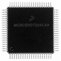
MC9S12XDT256CAA Freescale Semiconductor, MC9S12XDT256CAA Datasheet - Page 173

MC9S12XDT256CAA
Manufacturer Part Number
MC9S12XDT256CAA
Description
IC MCU 256K FLASH 80-QFP
Manufacturer
Freescale Semiconductor
Series
HCS12r
Datasheet
1.MC9S12XD64CAA.pdf
(1348 pages)
Specifications of MC9S12XDT256CAA
Core Processor
HCS12X
Core Size
16-Bit
Speed
80MHz
Connectivity
CAN, EBI/EMI, I²C, IrDA, LIN, SCI, SPI
Peripherals
LVD, POR, PWM, WDT
Number Of I /o
59
Program Memory Size
256KB (256K x 8)
Program Memory Type
FLASH
Eeprom Size
4K x 8
Ram Size
16K x 8
Voltage - Supply (vcc/vdd)
2.35 V ~ 5.5 V
Data Converters
A/D 8x10b
Oscillator Type
External
Operating Temperature
-40°C ~ 85°C
Package / Case
80-QFP
Processor Series
S12XD
Core
HCS12
Data Bus Width
16 bit
Data Ram Size
16 KB
Interface Type
CAN/I2C/SCI/SPI
Maximum Clock Frequency
40 MHz
Number Of Programmable I/os
59
Number Of Timers
12
Maximum Operating Temperature
+ 85 C
Mounting Style
SMD/SMT
3rd Party Development Tools
EWHCS12
Development Tools By Supplier
EVB9S12XDP512E
Minimum Operating Temperature
- 40 C
On-chip Adc
8-ch x 10-bit
Lead Free Status / RoHS Status
Lead free / RoHS Compliant
Available stocks
Company
Part Number
Manufacturer
Quantity
Price
Company:
Part Number:
MC9S12XDT256CAA
Manufacturer:
Freescale Semiconductor
Quantity:
10 000
Company:
Part Number:
MC9S12XDT256CAAR
Manufacturer:
Freescale Semiconductor
Quantity:
10 000
- Current page: 173 of 1348
- Download datasheet (8Mb)
5.3.2.6
This register selects the type of conversion sequence and the analog input channels sampled. Writes to this
register will abort current conversion sequence and start a new conversion sequence.
Read: Anytime
Write: Anytime
Freescale Semiconductor
CC, CB, CA
Reset
DSGN
SCAN
MULT
Field
DJM
2–0
7
6
5
4
W
R
DJM
Result Register Data Justification — This bit controls justification of conversion data in the result registers.
See
0 Left justified data in the result registers
1 Right justified data in the result registers
Result Register Data Signed or Unsigned Representation — This bit selects between signed and unsigned
conversion data representation in the result registers. Signed data is represented as 2’s complement. Signed
data is not available in right justification. See
for details.
0 Unsigned data representation in the result registers
1 Signed data representation in the result registers
Table 5-14
Table 5-15
signal range between 0 and 5.12 Volts.
Continuous Conversion Sequence Mode — This bit selects whether conversion sequences are performed
continuously or only once.
0 Single conversion sequence
1 Continuous conversion sequences (scan mode)
Multi-Channel Sample Mode — When MULT is 0, the ATD sequence controller samples only from the specified
analog input channel for an entire conversion sequence. The analog channel is selected by channel selection
code (control bits CC/CB/CA located in ATDCTL5). When MULT is 1, the ATD sequence controller samples
across channels. The number of channels sampled is determined by the sequence length value (S8C, S4C,
S2C, S1C). The first analog channel examined is determined by channel selection code (CC, CB, CA control
bits); subsequent channels sampled in the sequence are determined by incrementing the channel selection
code.
0 Sample only one channel
1 Sample across several channels
Analog Input Channel Select Code — These bits select the analog input channel(s) whose signals are
sampled and converted to digital codes.
channels. In the case of single channel scans (MULT = 0), this selection code specified the channel examined.
In the case of multi-channel scans (MULT = 1), this selection code represents the first channel to be examined
in the conversion sequence. Subsequent channels are determined by incrementing channel selection code;
selection codes that reach the maximum value wrap around to the minimum value.
ATD Control Register 5 (ATDCTL5)
0
7
Section 5.3.2.13, “ATD Conversion Result Registers (ATDDRx),”
= Unimplemented or Reserved
summarizes the result data formats available and how they are set up using the control bits.
illustrates the difference between the signed and unsigned, left justified output codes for an input
DSGN
0
6
Figure 5-8. ATD Control Register 5 (ATDCTL5)
Table 5-13. ATDCTL5 Field Descriptions
MC9S12XDP512 Data Sheet, Rev. 2.21
SCAN
0
5
Table 5-16
MULT
0
4
Section 5.3.2.13, “ATD Conversion Result Registers (ATDDRx),”
Description
lists the coding used to select the various analog input
Chapter 5 Analog-to-Digital Converter (S12ATD10B8CV2)
0
0
3
for details.
CC
0
2
CB
0
1
CA
0
0
173
Related parts for MC9S12XDT256CAA
Image
Part Number
Description
Manufacturer
Datasheet
Request
R

Part Number:
Description:
16-BIT MICROPROCESSOR FAMILY
Manufacturer:
FREESCALE [Freescale Semiconductor, Inc]
Datasheet:
Part Number:
Description:
Manufacturer:
Freescale Semiconductor, Inc
Datasheet:
Part Number:
Description:
Manufacturer:
Freescale Semiconductor, Inc
Datasheet:
Part Number:
Description:
Manufacturer:
Freescale Semiconductor, Inc
Datasheet:
Part Number:
Description:
Manufacturer:
Freescale Semiconductor, Inc
Datasheet:
Part Number:
Description:
Manufacturer:
Freescale Semiconductor, Inc
Datasheet:
Part Number:
Description:
Manufacturer:
Freescale Semiconductor, Inc
Datasheet:
Part Number:
Description:
Manufacturer:
Freescale Semiconductor, Inc
Datasheet:
Part Number:
Description:
Manufacturer:
Freescale Semiconductor, Inc
Datasheet:
Part Number:
Description:
Manufacturer:
Freescale Semiconductor, Inc
Datasheet:
Part Number:
Description:
Manufacturer:
Freescale Semiconductor, Inc
Datasheet:
Part Number:
Description:
Manufacturer:
Freescale Semiconductor, Inc
Datasheet:
Part Number:
Description:
Manufacturer:
Freescale Semiconductor, Inc
Datasheet:
Part Number:
Description:
Manufacturer:
Freescale Semiconductor, Inc
Datasheet:
Part Number:
Description:
Manufacturer:
Freescale Semiconductor, Inc
Datasheet:


