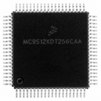
MC9S12XDT256CAA Freescale Semiconductor, MC9S12XDT256CAA Datasheet - Page 211

MC9S12XDT256CAA
Manufacturer Part Number
MC9S12XDT256CAA
Description
IC MCU 256K FLASH 80-QFP
Manufacturer
Freescale Semiconductor
Series
HCS12r
Datasheet
1.MC9S12XD64CAA.pdf
(1348 pages)
Specifications of MC9S12XDT256CAA
Core Processor
HCS12X
Core Size
16-Bit
Speed
80MHz
Connectivity
CAN, EBI/EMI, I²C, IrDA, LIN, SCI, SPI
Peripherals
LVD, POR, PWM, WDT
Number Of I /o
59
Program Memory Size
256KB (256K x 8)
Program Memory Type
FLASH
Eeprom Size
4K x 8
Ram Size
16K x 8
Voltage - Supply (vcc/vdd)
2.35 V ~ 5.5 V
Data Converters
A/D 8x10b
Oscillator Type
External
Operating Temperature
-40°C ~ 85°C
Package / Case
80-QFP
Processor Series
S12XD
Core
HCS12
Data Bus Width
16 bit
Data Ram Size
16 KB
Interface Type
CAN/I2C/SCI/SPI
Maximum Clock Frequency
40 MHz
Number Of Programmable I/os
59
Number Of Timers
12
Maximum Operating Temperature
+ 85 C
Mounting Style
SMD/SMT
3rd Party Development Tools
EWHCS12
Development Tools By Supplier
EVB9S12XDP512E
Minimum Operating Temperature
- 40 C
On-chip Adc
8-ch x 10-bit
Lead Free Status / RoHS Status
Lead free / RoHS Compliant
Available stocks
Company
Part Number
Manufacturer
Quantity
Price
Company:
Part Number:
MC9S12XDT256CAA
Manufacturer:
Freescale Semiconductor
Quantity:
10 000
Company:
Part Number:
MC9S12XDT256CAAR
Manufacturer:
Freescale Semiconductor
Quantity:
10 000
- Current page: 211 of 1348
- Download datasheet (8Mb)
6.8.1.8
In this mode the result of an operation between two registers is stored in one of the registers used as
operands.
RD = RD RS is the general register to register format, with register RD being the first operand and RS
the second. RD and RS can be any of the 8 general purpose registers R0 … R7. If R0 is used as the
destination register, only the condition code flags are updated. This addressing mode is used only for shift
operations with a variable shift value
Examples:
6.8.1.9
In this mode the result of an operation between two or three registers is stored into a third one.
RD = RS1 RS2 is the general format used in the order RD, RS1, RS1. RD, RS1, RS2 can be any of the
8 general purpose registers R0 … R7. If R0 is used as the destination register RD, only the condition code
flags are updated. This addressing mode is used for all arithmetic and logical operations.
Examples:
6.8.1.10
A 9-bit signed word address offset is included in the instruction word. This addressing mode is used for
conditional branch instructions.
Examples:
6.8.1.11
An 11-bit signed word address offset is included in the instruction word. This addressing mode is used for
the unconditional branch instruction.
Examples:
6.8.1.12
(RS, #offset5) provides an unsigned offset from the base register.
Examples:
Freescale Semiconductor
LSL
LSR
ADC
SUB
BCC
BEQ
BRA
LDB
STW
Dyadic Addressing (DYA)
Triadic Addressing (TRI)
Relative Addressing 9-Bit Wide (REL9)
Relative Addressing 10-Bit Wide (REL10)
Index Register plus Immediate Offset (IDO5)
R4,R5
R4,R5
R5,R6,R7
R5,R6,R7
REL9
REL9
REL10
R4,(R1,#offset)
R4,(R1,#offset)
; R4 = R4 << R5
; R4 = R4 >> R5
MC9S12XDP512 Data Sheet, Rev. 2.21
; R5 = R6 + R7 + Carry
; R5 = R6 - R7
; PC = PC + 2 + (REL9 << 1)
; PC = PC + 2 + (REL9 << 1)
; PC = PC + 2 + (REL10 << 1)
; loads a byte from R1+offset into R4
; stores R4 as a word to R1+offset
Chapter 6 XGATE (S12XGATEV2)
211
Related parts for MC9S12XDT256CAA
Image
Part Number
Description
Manufacturer
Datasheet
Request
R

Part Number:
Description:
16-BIT MICROPROCESSOR FAMILY
Manufacturer:
FREESCALE [Freescale Semiconductor, Inc]
Datasheet:
Part Number:
Description:
Manufacturer:
Freescale Semiconductor, Inc
Datasheet:
Part Number:
Description:
Manufacturer:
Freescale Semiconductor, Inc
Datasheet:
Part Number:
Description:
Manufacturer:
Freescale Semiconductor, Inc
Datasheet:
Part Number:
Description:
Manufacturer:
Freescale Semiconductor, Inc
Datasheet:
Part Number:
Description:
Manufacturer:
Freescale Semiconductor, Inc
Datasheet:
Part Number:
Description:
Manufacturer:
Freescale Semiconductor, Inc
Datasheet:
Part Number:
Description:
Manufacturer:
Freescale Semiconductor, Inc
Datasheet:
Part Number:
Description:
Manufacturer:
Freescale Semiconductor, Inc
Datasheet:
Part Number:
Description:
Manufacturer:
Freescale Semiconductor, Inc
Datasheet:
Part Number:
Description:
Manufacturer:
Freescale Semiconductor, Inc
Datasheet:
Part Number:
Description:
Manufacturer:
Freescale Semiconductor, Inc
Datasheet:
Part Number:
Description:
Manufacturer:
Freescale Semiconductor, Inc
Datasheet:
Part Number:
Description:
Manufacturer:
Freescale Semiconductor, Inc
Datasheet:
Part Number:
Description:
Manufacturer:
Freescale Semiconductor, Inc
Datasheet:


