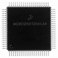
MC9S12XDT256CAA Freescale Semiconductor, MC9S12XDT256CAA Datasheet - Page 359

MC9S12XDT256CAA
Manufacturer Part Number
MC9S12XDT256CAA
Description
IC MCU 256K FLASH 80-QFP
Manufacturer
Freescale Semiconductor
Series
HCS12r
Datasheet
1.MC9S12XD64CAA.pdf
(1348 pages)
Specifications of MC9S12XDT256CAA
Core Processor
HCS12X
Core Size
16-Bit
Speed
80MHz
Connectivity
CAN, EBI/EMI, I²C, IrDA, LIN, SCI, SPI
Peripherals
LVD, POR, PWM, WDT
Number Of I /o
59
Program Memory Size
256KB (256K x 8)
Program Memory Type
FLASH
Eeprom Size
4K x 8
Ram Size
16K x 8
Voltage - Supply (vcc/vdd)
2.35 V ~ 5.5 V
Data Converters
A/D 8x10b
Oscillator Type
External
Operating Temperature
-40°C ~ 85°C
Package / Case
80-QFP
Processor Series
S12XD
Core
HCS12
Data Bus Width
16 bit
Data Ram Size
16 KB
Interface Type
CAN/I2C/SCI/SPI
Maximum Clock Frequency
40 MHz
Number Of Programmable I/os
59
Number Of Timers
12
Maximum Operating Temperature
+ 85 C
Mounting Style
SMD/SMT
3rd Party Development Tools
EWHCS12
Development Tools By Supplier
EVB9S12XDP512E
Minimum Operating Temperature
- 40 C
On-chip Adc
8-ch x 10-bit
Lead Free Status / RoHS Status
Lead free / RoHS Compliant
Available stocks
Company
Part Number
Manufacturer
Quantity
Price
Company:
Part Number:
MC9S12XDT256CAA
Manufacturer:
Freescale Semiconductor
Quantity:
10 000
Company:
Part Number:
MC9S12XDT256CAAR
Manufacturer:
Freescale Semiconductor
Quantity:
10 000
- Current page: 359 of 1348
- Download datasheet (8Mb)
7.4.1.2
Internal register whose output drives OCx when TIOS is set, can be force loaded with a desired data by
writing to CFORC register before OCx is configured for output compare action. This allows a glitch free
switch over of port from general purpose I/O to timer output once the output compare is enabled.
7.4.1.3
There are four 8-bit pulse accumulators with four 8-bit holding registers associated with the four IC
buffered channels 3–0. A pulse accumulator counts the number of active edges at the input of its channel.
The minimum pulse width for the PAI input is greater than two bus clocks.The maximum input frequency
on the pulse accumulator channel is one half the bus frequency or Eclk.
The user can prevent the 8-bit pulse accumulators from counting further than 0x00FF by utilizing the
PACMX control bit in the ICSYS register. In this case, a value of 0x00FF means that 255 counts or more
have occurred.
Each pair of pulse accumulators can be used as a 16-bit pulse accumulator (see
Pulse accumulator B operates only as an event counter, it does not feature gated time accumulation
mode.The edge control for pulse accumulator B as a 16-bit pulse accumulator is defined by TCTL4[1:0].
To operate the 16-bit pulse accumulators A and B (PACA and PACB) independently of input capture or
output compare 7 and 0 respectively, the user must set the corresponding bits: IOSx = 1, OMx = 0, and
OLx = 0. OC7M7 or OC7M0 in the OC7M register must also be cleared.
There are two modes of operation for the pulse accumulators:
7.4.1.4
The modulus down-counter can be used as a time base to generate a periodic interrupt. It can also be used
to latch the values of the IC registers and the pulse accumulators to their holding registers.
The action of latching can be programmed to be periodic or only once.
Freescale Semiconductor
•
•
Pulse accumulator latch mode
The value of the pulse accumulator is transferred to its holding register when the modulus
down-counter reaches zero, a write 0x0000 to the modulus counter or when the force latch control
bit ICLAT is written.
At the same time the pulse accumulator is cleared.
Pulse accumulator queue mode
When queue mode is enabled, reads of an input capture holding register will transfer the contents
of the associated pulse accumulator to its holding register.
At the same time the pulse accumulator is cleared.
OC Channel Initialization
Pulse Accumulators
Modulus Down-Counter
MC9S12XDP512 Data Sheet, Rev. 2.21
Chapter 7 Enhanced Capture Timer (S12ECT16B8CV2)
Figure
7-70).
359
Related parts for MC9S12XDT256CAA
Image
Part Number
Description
Manufacturer
Datasheet
Request
R

Part Number:
Description:
16-BIT MICROPROCESSOR FAMILY
Manufacturer:
FREESCALE [Freescale Semiconductor, Inc]
Datasheet:
Part Number:
Description:
Manufacturer:
Freescale Semiconductor, Inc
Datasheet:
Part Number:
Description:
Manufacturer:
Freescale Semiconductor, Inc
Datasheet:
Part Number:
Description:
Manufacturer:
Freescale Semiconductor, Inc
Datasheet:
Part Number:
Description:
Manufacturer:
Freescale Semiconductor, Inc
Datasheet:
Part Number:
Description:
Manufacturer:
Freescale Semiconductor, Inc
Datasheet:
Part Number:
Description:
Manufacturer:
Freescale Semiconductor, Inc
Datasheet:
Part Number:
Description:
Manufacturer:
Freescale Semiconductor, Inc
Datasheet:
Part Number:
Description:
Manufacturer:
Freescale Semiconductor, Inc
Datasheet:
Part Number:
Description:
Manufacturer:
Freescale Semiconductor, Inc
Datasheet:
Part Number:
Description:
Manufacturer:
Freescale Semiconductor, Inc
Datasheet:
Part Number:
Description:
Manufacturer:
Freescale Semiconductor, Inc
Datasheet:
Part Number:
Description:
Manufacturer:
Freescale Semiconductor, Inc
Datasheet:
Part Number:
Description:
Manufacturer:
Freescale Semiconductor, Inc
Datasheet:
Part Number:
Description:
Manufacturer:
Freescale Semiconductor, Inc
Datasheet:


