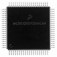
MC9S12XDT256CAA Freescale Semiconductor, MC9S12XDT256CAA Datasheet - Page 372

MC9S12XDT256CAA
Manufacturer Part Number
MC9S12XDT256CAA
Description
IC MCU 256K FLASH 80-QFP
Manufacturer
Freescale Semiconductor
Series
HCS12r
Datasheet
1.MC9S12XD64CAA.pdf
(1348 pages)
Specifications of MC9S12XDT256CAA
Core Processor
HCS12X
Core Size
16-Bit
Speed
80MHz
Connectivity
CAN, EBI/EMI, I²C, IrDA, LIN, SCI, SPI
Peripherals
LVD, POR, PWM, WDT
Number Of I /o
59
Program Memory Size
256KB (256K x 8)
Program Memory Type
FLASH
Eeprom Size
4K x 8
Ram Size
16K x 8
Voltage - Supply (vcc/vdd)
2.35 V ~ 5.5 V
Data Converters
A/D 8x10b
Oscillator Type
External
Operating Temperature
-40°C ~ 85°C
Package / Case
80-QFP
Processor Series
S12XD
Core
HCS12
Data Bus Width
16 bit
Data Ram Size
16 KB
Interface Type
CAN/I2C/SCI/SPI
Maximum Clock Frequency
40 MHz
Number Of Programmable I/os
59
Number Of Timers
12
Maximum Operating Temperature
+ 85 C
Mounting Style
SMD/SMT
3rd Party Development Tools
EWHCS12
Development Tools By Supplier
EVB9S12XDP512E
Minimum Operating Temperature
- 40 C
On-chip Adc
8-ch x 10-bit
Lead Free Status / RoHS Status
Lead free / RoHS Compliant
Available stocks
Company
Part Number
Manufacturer
Quantity
Price
Company:
Part Number:
MC9S12XDT256CAA
Manufacturer:
Freescale Semiconductor
Quantity:
10 000
Company:
Part Number:
MC9S12XDT256CAAR
Manufacturer:
Freescale Semiconductor
Quantity:
10 000
- Current page: 372 of 1348
- Download datasheet (8Mb)
Chapter 8 Pulse-Width Modulator (S12PWM8B8CV1)
8.3.2.5
The PWMCAE register contains eight control bits for the selection of center aligned outputs or left aligned
outputs for each PWM channel. If the CAEx bit is set to a one, the corresponding PWM output will be
center aligned. If the CAEx bit is cleared, the corresponding PWM output will be left aligned. See
Section 8.4.2.5, “Left Aligned Outputs”
description of the PWM output modes.
372
PCKB[2:0]
PCKA[2:0]
s
Reset
Field
6–4
2–0
W
R
CAE7
Prescaler Select for Clock B — Clock B is one of two clock sources which can be used for channels 2, 3, 6, or
7. These three bits determine the rate of clock B, as shown in
Prescaler Select for Clock A — Clock A is one of two clock sources which can be used for channels 0, 1, 4 or
5. These three bits determine the rate of clock A, as shown in
PWM Center Align Enable Register (PWMCAE)
0
7
PCKB2–0 and PCKA2–0 register bits can be written anytime. If the clock
pre-scale is changed while a PWM signal is being generated, a truncated or
stretched pulse can occur during the transition.
CAE6
Figure 8-7. PWM Center Align Enable Register (PWMCAE)
PCKB2
PCKA2
0
6
0
0
0
0
1
1
1
1
0
0
0
0
1
1
1
1
Table 8-4. PWMPRCLK Field Descriptions
Table 8-5. Clock B Prescaler Selects
Table 8-6. Clock A Prescaler Selects
MC9S12XDP512 Data Sheet, Rev. 2.21
CAE5
PCKB1
PCKA1
0
5
and
0
0
1
1
0
0
1
1
0
0
1
1
0
0
1
1
Section 8.4.2.6, “Center Aligned Outputs”
CAE4
NOTE
PCKB0
0
PCKA0
4
0
1
0
1
0
1
0
1
0
1
0
1
0
1
0
1
Description
CAE3
0
3
Value of Clock B
Value of Clock A
Table
Table
Bus clock / 128
Bus clock / 128
Bus clock / 16
Bus clock / 32
Bus clock / 16
Bus clock / 32
Bus clock / 64
Bus clock / 64
Bus clock / 2
Bus clock / 4
Bus clock / 8
Bus clock / 2
Bus clock / 4
Bus clock / 8
Bus clock
Bus clock
8-5.
8-6.
CAE2
0
2
Freescale Semiconductor
CAE1
for a more detailed
0
1
CAE0
0
0
Related parts for MC9S12XDT256CAA
Image
Part Number
Description
Manufacturer
Datasheet
Request
R

Part Number:
Description:
16-BIT MICROPROCESSOR FAMILY
Manufacturer:
FREESCALE [Freescale Semiconductor, Inc]
Datasheet:
Part Number:
Description:
Manufacturer:
Freescale Semiconductor, Inc
Datasheet:
Part Number:
Description:
Manufacturer:
Freescale Semiconductor, Inc
Datasheet:
Part Number:
Description:
Manufacturer:
Freescale Semiconductor, Inc
Datasheet:
Part Number:
Description:
Manufacturer:
Freescale Semiconductor, Inc
Datasheet:
Part Number:
Description:
Manufacturer:
Freescale Semiconductor, Inc
Datasheet:
Part Number:
Description:
Manufacturer:
Freescale Semiconductor, Inc
Datasheet:
Part Number:
Description:
Manufacturer:
Freescale Semiconductor, Inc
Datasheet:
Part Number:
Description:
Manufacturer:
Freescale Semiconductor, Inc
Datasheet:
Part Number:
Description:
Manufacturer:
Freescale Semiconductor, Inc
Datasheet:
Part Number:
Description:
Manufacturer:
Freescale Semiconductor, Inc
Datasheet:
Part Number:
Description:
Manufacturer:
Freescale Semiconductor, Inc
Datasheet:
Part Number:
Description:
Manufacturer:
Freescale Semiconductor, Inc
Datasheet:
Part Number:
Description:
Manufacturer:
Freescale Semiconductor, Inc
Datasheet:
Part Number:
Description:
Manufacturer:
Freescale Semiconductor, Inc
Datasheet:


