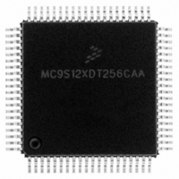
MC9S12XDT256CAA Freescale Semiconductor, MC9S12XDT256CAA Datasheet - Page 383

MC9S12XDT256CAA
Manufacturer Part Number
MC9S12XDT256CAA
Description
IC MCU 256K FLASH 80-QFP
Manufacturer
Freescale Semiconductor
Series
HCS12r
Datasheet
1.MC9S12XD64CAA.pdf
(1348 pages)
Specifications of MC9S12XDT256CAA
Core Processor
HCS12X
Core Size
16-Bit
Speed
80MHz
Connectivity
CAN, EBI/EMI, I²C, IrDA, LIN, SCI, SPI
Peripherals
LVD, POR, PWM, WDT
Number Of I /o
59
Program Memory Size
256KB (256K x 8)
Program Memory Type
FLASH
Eeprom Size
4K x 8
Ram Size
16K x 8
Voltage - Supply (vcc/vdd)
2.35 V ~ 5.5 V
Data Converters
A/D 8x10b
Oscillator Type
External
Operating Temperature
-40°C ~ 85°C
Package / Case
80-QFP
Processor Series
S12XD
Core
HCS12
Data Bus Width
16 bit
Data Ram Size
16 KB
Interface Type
CAN/I2C/SCI/SPI
Maximum Clock Frequency
40 MHz
Number Of Programmable I/os
59
Number Of Timers
12
Maximum Operating Temperature
+ 85 C
Mounting Style
SMD/SMT
3rd Party Development Tools
EWHCS12
Development Tools By Supplier
EVB9S12XDP512E
Minimum Operating Temperature
- 40 C
On-chip Adc
8-ch x 10-bit
Lead Free Status / RoHS Status
Lead free / RoHS Compliant
Available stocks
Company
Part Number
Manufacturer
Quantity
Price
Company:
Part Number:
MC9S12XDT256CAA
Manufacturer:
Freescale Semiconductor
Quantity:
10 000
Company:
Part Number:
MC9S12XDT256CAAR
Manufacturer:
Freescale Semiconductor
Quantity:
10 000
- Current page: 383 of 1348
- Download datasheet (8Mb)
Clock A is used as an input to an 8-bit down counter. This down counter loads a user programmable scale
value from the scale register (PWMSCLA). When the down counter reaches one, a pulse is output and the
8-bit counter is re-loaded. The output signal from this circuit is further divided by two. This gives a greater
range with only a slight reduction in granularity. Clock SA equals clock A divided by two times the value
in the PWMSCLA register.
Similarly, clock B is used as an input to an 8-bit down counter followed by a divide by two producing clock
SB. Thus, clock SB equals clock B divided by two times the value in the PWMSCLB register.
As an example, consider the case in which the user writes $FF into the PWMSCLA register. Clock A for
this case will be E divided by 4. A pulse will occur at a rate of once every 255x4 E cycles. Passing this
through the divide by two circuit produces a clock signal at an E divided by 2040 rate. Similarly, a value
of $01 in the PWMSCLA register when clock A is E divided by 4 will produce a clock at an E divided by
8 rate.
Otherwise, when changing rates the counter would have to count down to $01 before counting at the proper
rate. Forcing the associated counter to re-load the scale register value every time PWMSCLA or
PWMSCLB is written prevents this.
8.4.1.3
Each PWM channel has the capability of selecting one of two clocks. For channels 0, 1, 4, and 5 the clock
choices are clock A or clock SA. For channels 2, 3, 6, and 7 the choices are clock B or clock SB. The clock
selection is done with the PCLKx control bits in the PWMCLK register.
Freescale Semiconductor
Writing to PWMSCLA or PWMSCLB causes the associated 8-bit down counter to be re-loaded.
Clock Select
Clock SA = Clock A / (2 * PWMSCLA)
When PWMSCLA = $00, PWMSCLA value is considered a full scale value
of 256. Clock A is thus divided by 512.
Clock SB = Clock B / (2 * PWMSCLB)
When PWMSCLB = $00, PWMSCLB value is considered a full scale value
of 256. Clock B is thus divided by 512.
Writing to the scale registers while channels are operating can cause
irregularities in the PWM outputs.
Changing clock control bits while channels are operating can cause
irregularities in the PWM outputs.
MC9S12XDP512 Data Sheet, Rev. 2.21
NOTE
NOTE
NOTE
NOTE
Chapter 8 Pulse-Width Modulator (S12PWM8B8CV1)
383
Related parts for MC9S12XDT256CAA
Image
Part Number
Description
Manufacturer
Datasheet
Request
R

Part Number:
Description:
16-BIT MICROPROCESSOR FAMILY
Manufacturer:
FREESCALE [Freescale Semiconductor, Inc]
Datasheet:
Part Number:
Description:
Manufacturer:
Freescale Semiconductor, Inc
Datasheet:
Part Number:
Description:
Manufacturer:
Freescale Semiconductor, Inc
Datasheet:
Part Number:
Description:
Manufacturer:
Freescale Semiconductor, Inc
Datasheet:
Part Number:
Description:
Manufacturer:
Freescale Semiconductor, Inc
Datasheet:
Part Number:
Description:
Manufacturer:
Freescale Semiconductor, Inc
Datasheet:
Part Number:
Description:
Manufacturer:
Freescale Semiconductor, Inc
Datasheet:
Part Number:
Description:
Manufacturer:
Freescale Semiconductor, Inc
Datasheet:
Part Number:
Description:
Manufacturer:
Freescale Semiconductor, Inc
Datasheet:
Part Number:
Description:
Manufacturer:
Freescale Semiconductor, Inc
Datasheet:
Part Number:
Description:
Manufacturer:
Freescale Semiconductor, Inc
Datasheet:
Part Number:
Description:
Manufacturer:
Freescale Semiconductor, Inc
Datasheet:
Part Number:
Description:
Manufacturer:
Freescale Semiconductor, Inc
Datasheet:
Part Number:
Description:
Manufacturer:
Freescale Semiconductor, Inc
Datasheet:
Part Number:
Description:
Manufacturer:
Freescale Semiconductor, Inc
Datasheet:


