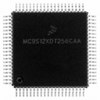
MC9S12XDT256CAA Freescale Semiconductor, MC9S12XDT256CAA Datasheet - Page 55

MC9S12XDT256CAA
Manufacturer Part Number
MC9S12XDT256CAA
Description
IC MCU 256K FLASH 80-QFP
Manufacturer
Freescale Semiconductor
Series
HCS12r
Datasheet
1.MC9S12XD64CAA.pdf
(1348 pages)
Specifications of MC9S12XDT256CAA
Core Processor
HCS12X
Core Size
16-Bit
Speed
80MHz
Connectivity
CAN, EBI/EMI, I²C, IrDA, LIN, SCI, SPI
Peripherals
LVD, POR, PWM, WDT
Number Of I /o
59
Program Memory Size
256KB (256K x 8)
Program Memory Type
FLASH
Eeprom Size
4K x 8
Ram Size
16K x 8
Voltage - Supply (vcc/vdd)
2.35 V ~ 5.5 V
Data Converters
A/D 8x10b
Oscillator Type
External
Operating Temperature
-40°C ~ 85°C
Package / Case
80-QFP
Processor Series
S12XD
Core
HCS12
Data Bus Width
16 bit
Data Ram Size
16 KB
Interface Type
CAN/I2C/SCI/SPI
Maximum Clock Frequency
40 MHz
Number Of Programmable I/os
59
Number Of Timers
12
Maximum Operating Temperature
+ 85 C
Mounting Style
SMD/SMT
3rd Party Development Tools
EWHCS12
Development Tools By Supplier
EVB9S12XDP512E
Minimum Operating Temperature
- 40 C
On-chip Adc
8-ch x 10-bit
Lead Free Status / RoHS Status
Lead free / RoHS Compliant
Available stocks
Company
Part Number
Manufacturer
Quantity
Price
Company:
Part Number:
MC9S12XDT256CAA
Manufacturer:
Freescale Semiconductor
Quantity:
10 000
Company:
Part Number:
MC9S12XDT256CAAR
Manufacturer:
Freescale Semiconductor
Quantity:
10 000
- Current page: 55 of 1348
- Download datasheet (8Mb)
1.2.3
1.2.3.1
EXTAL and XTAL are the crystal driver and external clock pins. On reset all the device clocks are derived
from the EXTAL input frequency. XTAL is the crystal output.
1.2.3.2
The RESET pin is an active low bidirectional control signal. It acts as an input to initialize the MCU to a
known start-up state. As an output it is driven ;ow to indicate when any internal MCU reset source triggers.
The RESET pin has an internal pullup device.
Freescale Semiconductor
Function 1
PT[7:0]
Name
PS5
PS4
PS3
PS2
PS1
PS0
Pin
Function 2
Detailed Signal Descriptions
IOC[7:0]
MOSI0
MISO0
Name
RXD1
RXD0
EXTAL, XTAL — Oscillator Pins
RESET — External Reset Pin
TXD1
TXD0
Pin
For devices assembled in 80-pin and 112-pin packages all non-bonded out
pins should be configured as outputs after reset in order to avoid current
drawn from floating inputs. Refer to
This section describes all pins which are availabe on the cover part
MC9S12XDP512 in 144-pin LQFP package. For modules and pinout
explanations of the different family members refer to
explanations:
Sets S12XA & S12XB - Family
Function 3
Name
Pin
—
—
—
—
—
—
—
Table 1-7. Signal Properties Summary (Sheet 4 of 4)
and
Function 4
E.5 Peripheral Sets S12XD - Family
Name
MC9S12XDP512 Data Sheet, Rev. 2.21
Pin
—
—
—
—
—
—
—
Function 5
Name
Pin
—
—
—
—
—
—
—
NOTE
NOTE
Table 1-7
Supply
Power
V
V
V
V
V
V
V
DDX
DDX
DDX
DDX
DDX
DDX
DDX
for affected pins.
PERS/
PERS/
PERS/
PERS/
PERS/
PERS/
PERT/
CTRL
PPSS
PPSS
PPSS
PPSS
PPSS
PPSS
PPST
Internal Pull
Resistor
Chapter 1 Device Overview MC9S12XD-Family
E.7 Pinout
and
Disabled Port T I/O, timer channels
Reset
State
E.6 Peripheral
Up
Up
Up
Up
Up
Up
Port S I/O, MOSI of SPI0
Port S I/O, MISO of SPI0
Port S I/O, TXD of SCI1
Port S I/O, RXD of SCI1
Port S I/O, TXD of SCI0
Port S I/O, RXD of SCI0
Description
55
Related parts for MC9S12XDT256CAA
Image
Part Number
Description
Manufacturer
Datasheet
Request
R

Part Number:
Description:
16-BIT MICROPROCESSOR FAMILY
Manufacturer:
FREESCALE [Freescale Semiconductor, Inc]
Datasheet:
Part Number:
Description:
Manufacturer:
Freescale Semiconductor, Inc
Datasheet:
Part Number:
Description:
Manufacturer:
Freescale Semiconductor, Inc
Datasheet:
Part Number:
Description:
Manufacturer:
Freescale Semiconductor, Inc
Datasheet:
Part Number:
Description:
Manufacturer:
Freescale Semiconductor, Inc
Datasheet:
Part Number:
Description:
Manufacturer:
Freescale Semiconductor, Inc
Datasheet:
Part Number:
Description:
Manufacturer:
Freescale Semiconductor, Inc
Datasheet:
Part Number:
Description:
Manufacturer:
Freescale Semiconductor, Inc
Datasheet:
Part Number:
Description:
Manufacturer:
Freescale Semiconductor, Inc
Datasheet:
Part Number:
Description:
Manufacturer:
Freescale Semiconductor, Inc
Datasheet:
Part Number:
Description:
Manufacturer:
Freescale Semiconductor, Inc
Datasheet:
Part Number:
Description:
Manufacturer:
Freescale Semiconductor, Inc
Datasheet:
Part Number:
Description:
Manufacturer:
Freescale Semiconductor, Inc
Datasheet:
Part Number:
Description:
Manufacturer:
Freescale Semiconductor, Inc
Datasheet:
Part Number:
Description:
Manufacturer:
Freescale Semiconductor, Inc
Datasheet:


