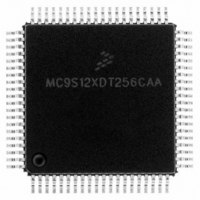
MC9S12XDT256CAA Freescale Semiconductor, MC9S12XDT256CAA Datasheet - Page 587

MC9S12XDT256CAA
Manufacturer Part Number
MC9S12XDT256CAA
Description
IC MCU 256K FLASH 80-QFP
Manufacturer
Freescale Semiconductor
Series
HCS12r
Datasheet
1.MC9S12XD64CAA.pdf
(1348 pages)
Specifications of MC9S12XDT256CAA
Core Processor
HCS12X
Core Size
16-Bit
Speed
80MHz
Connectivity
CAN, EBI/EMI, I²C, IrDA, LIN, SCI, SPI
Peripherals
LVD, POR, PWM, WDT
Number Of I /o
59
Program Memory Size
256KB (256K x 8)
Program Memory Type
FLASH
Eeprom Size
4K x 8
Ram Size
16K x 8
Voltage - Supply (vcc/vdd)
2.35 V ~ 5.5 V
Data Converters
A/D 8x10b
Oscillator Type
External
Operating Temperature
-40°C ~ 85°C
Package / Case
80-QFP
Processor Series
S12XD
Core
HCS12
Data Bus Width
16 bit
Data Ram Size
16 KB
Interface Type
CAN/I2C/SCI/SPI
Maximum Clock Frequency
40 MHz
Number Of Programmable I/os
59
Number Of Timers
12
Maximum Operating Temperature
+ 85 C
Mounting Style
SMD/SMT
3rd Party Development Tools
EWHCS12
Development Tools By Supplier
EVB9S12XDP512E
Minimum Operating Temperature
- 40 C
On-chip Adc
8-ch x 10-bit
Lead Free Status / RoHS Status
Lead free / RoHS Compliant
Available stocks
Company
Part Number
Manufacturer
Quantity
Price
Company:
Part Number:
MC9S12XDT256CAA
Manufacturer:
Freescale Semiconductor
Quantity:
10 000
Company:
Part Number:
MC9S12XDT256CAAR
Manufacturer:
Freescale Semiconductor
Quantity:
10 000
- Current page: 587 of 1348
- Download datasheet (8Mb)
compared to the serial communication rate. This protocol allows a great flexibility for the POD designers,
since it does not rely on any accurate time measurement or short response time to any event in the serial
communication.
Figure 15-12
instruction is used as an example. First, the 8-bit instruction opcode is sent by the host, followed by the
address of the memory location to be read. The target BDM decodes the instruction. A bus cycle is grabbed
(free or stolen) by the BDM and it executes the READ_BYTE operation. Having retrieved the data, the
BDM issues an ACK pulse to the host controller, indicating that the addressed byte is ready to be retrieved.
After detecting the ACK pulse, the host initiates the byte retrieval process. Note that data is sent in the form
of a word and the host needs to determine which is the appropriate byte based on whether the address was
odd or even.
Freescale Semiconductor
BKGD Pin
(Target MCU)
ACK Pulse
BDM Clock
BKGD Pin
Transmits
Last Command Bit
16th Tick of the
Target
shows the ACK handshake protocol in a command level timing diagram. The READ_BYTE
READ_BYTE
If the ACK pulse was issued by the target, the host assumes the previous
command was executed. If the CPU enters wait or stop prior to executing a
hardware command, the ACK pulse will not be issued meaning that the
BDM command was not executed. After entering wait or stop mode, the
BDM command is no longer pending.
Host
Figure 15-12. Handshake Protocol at Command Level
High-Impedance
Byte Address
32 Cycles
Target
Figure 15-11. Target Acknowledge Pulse (ACK)
BDM Decodes
the Command
MC9S12XDP512 Data Sheet, Rev. 2.21
Minimum Delay
From the BDM Command
NOTE
16 Cycles
READ_BYTE Command
BDM Executes the
Chapter 15 Background Debug Module (S12XBDMV2)
Speedup Pulse
Target
BDM Issues the
ACK Pulse (out of scale)
(2) Bytes are
Retrieved
Host
Next Bit
Earliest
Start of
High-Impedance
Host
Command
New BDM
Target
587
Related parts for MC9S12XDT256CAA
Image
Part Number
Description
Manufacturer
Datasheet
Request
R

Part Number:
Description:
16-BIT MICROPROCESSOR FAMILY
Manufacturer:
FREESCALE [Freescale Semiconductor, Inc]
Datasheet:
Part Number:
Description:
Manufacturer:
Freescale Semiconductor, Inc
Datasheet:
Part Number:
Description:
Manufacturer:
Freescale Semiconductor, Inc
Datasheet:
Part Number:
Description:
Manufacturer:
Freescale Semiconductor, Inc
Datasheet:
Part Number:
Description:
Manufacturer:
Freescale Semiconductor, Inc
Datasheet:
Part Number:
Description:
Manufacturer:
Freescale Semiconductor, Inc
Datasheet:
Part Number:
Description:
Manufacturer:
Freescale Semiconductor, Inc
Datasheet:
Part Number:
Description:
Manufacturer:
Freescale Semiconductor, Inc
Datasheet:
Part Number:
Description:
Manufacturer:
Freescale Semiconductor, Inc
Datasheet:
Part Number:
Description:
Manufacturer:
Freescale Semiconductor, Inc
Datasheet:
Part Number:
Description:
Manufacturer:
Freescale Semiconductor, Inc
Datasheet:
Part Number:
Description:
Manufacturer:
Freescale Semiconductor, Inc
Datasheet:
Part Number:
Description:
Manufacturer:
Freescale Semiconductor, Inc
Datasheet:
Part Number:
Description:
Manufacturer:
Freescale Semiconductor, Inc
Datasheet:
Part Number:
Description:
Manufacturer:
Freescale Semiconductor, Inc
Datasheet:


