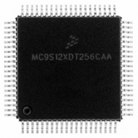
MC9S12XDT256CAA Freescale Semiconductor, MC9S12XDT256CAA Datasheet - Page 630

MC9S12XDT256CAA
Manufacturer Part Number
MC9S12XDT256CAA
Description
IC MCU 256K FLASH 80-QFP
Manufacturer
Freescale Semiconductor
Series
HCS12r
Datasheet
1.MC9S12XD64CAA.pdf
(1348 pages)
Specifications of MC9S12XDT256CAA
Core Processor
HCS12X
Core Size
16-Bit
Speed
80MHz
Connectivity
CAN, EBI/EMI, I²C, IrDA, LIN, SCI, SPI
Peripherals
LVD, POR, PWM, WDT
Number Of I /o
59
Program Memory Size
256KB (256K x 8)
Program Memory Type
FLASH
Eeprom Size
4K x 8
Ram Size
16K x 8
Voltage - Supply (vcc/vdd)
2.35 V ~ 5.5 V
Data Converters
A/D 8x10b
Oscillator Type
External
Operating Temperature
-40°C ~ 85°C
Package / Case
80-QFP
Processor Series
S12XD
Core
HCS12
Data Bus Width
16 bit
Data Ram Size
16 KB
Interface Type
CAN/I2C/SCI/SPI
Maximum Clock Frequency
40 MHz
Number Of Programmable I/os
59
Number Of Timers
12
Maximum Operating Temperature
+ 85 C
Mounting Style
SMD/SMT
3rd Party Development Tools
EWHCS12
Development Tools By Supplier
EVB9S12XDP512E
Minimum Operating Temperature
- 40 C
On-chip Adc
8-ch x 10-bit
Lead Free Status / RoHS Status
Lead free / RoHS Compliant
Available stocks
Company
Part Number
Manufacturer
Quantity
Price
Company:
Part Number:
MC9S12XDT256CAA
Manufacturer:
Freescale Semiconductor
Quantity:
10 000
Company:
Part Number:
MC9S12XDT256CAAR
Manufacturer:
Freescale Semiconductor
Quantity:
10 000
- Current page: 630 of 1348
- Download datasheet (8Mb)
Chapter 17 Memory Mapping Control (S12XMMCV2)
17.3.2.12 RAM Shared Region Upper Boundary Register (RAMSHU)
Read: Anytime
Write: Anytime when RWPE = 0
17.4
The MMC block performs several basic functions of the S12X sub-system operation: MCU operation
modes, priority control, address mapping, select signal generation and access limitations for the system.
Each aspect is described in the following subsections.
17.4.1
630
Address: 0x011F
SHU[6:0]
Reset
•
•
•
Field
6–0
W
R
Normal single-chip mode
There is no external bus in this mode. The MCU program is executed from the internal memory
and no external accesses are allowed.
Special single-chip mode
This mode is generally used for debugging single-chip operation, boot-strapping or security related
operations. The active background debug mode is in control of the CPU code execution and the
BDM firmware is waiting for serial commands sent through the BKGD pin. There is no external
bus in this mode.
Emulation single-chip mode
Tool vendors use this mode for emulation systems in which the user’s target application is normal
single-chip mode. Code is executed from external or internal memory depending on the set-up of
the EROMON bit (see
is active in both cases to allow observation of internal operations (internal visibility).
Functional Description
MCU Operating Mode
RAM Shared Region Upper Boundary Bits 6–0 — These bits define the upper boundary of the shared
memory in multiples of 256 bytes. The block selected by this register is included in the region. See
for details.
1
1
7
Figure 17-20. RAM Shared Region Upper Boundary Register (RAMSHU)
= Unimplemented or Reserved
SHU6
1
6
Section 1.3.2.5, “MMC Control Register
Table 17-17. RAMSHU Field Descriptions
MC9S12XDP512 Data Sheet, Rev. 2.21
SHU5
1
5
SHU4
1
4
Description
SHU3
1
3
(MMCCTL1)”). The external bus
SHU2
1
2
Freescale Semiconductor
SHU1
1
1
Figure 1-25
SHU0
1
0
Related parts for MC9S12XDT256CAA
Image
Part Number
Description
Manufacturer
Datasheet
Request
R

Part Number:
Description:
16-BIT MICROPROCESSOR FAMILY
Manufacturer:
FREESCALE [Freescale Semiconductor, Inc]
Datasheet:
Part Number:
Description:
Manufacturer:
Freescale Semiconductor, Inc
Datasheet:
Part Number:
Description:
Manufacturer:
Freescale Semiconductor, Inc
Datasheet:
Part Number:
Description:
Manufacturer:
Freescale Semiconductor, Inc
Datasheet:
Part Number:
Description:
Manufacturer:
Freescale Semiconductor, Inc
Datasheet:
Part Number:
Description:
Manufacturer:
Freescale Semiconductor, Inc
Datasheet:
Part Number:
Description:
Manufacturer:
Freescale Semiconductor, Inc
Datasheet:
Part Number:
Description:
Manufacturer:
Freescale Semiconductor, Inc
Datasheet:
Part Number:
Description:
Manufacturer:
Freescale Semiconductor, Inc
Datasheet:
Part Number:
Description:
Manufacturer:
Freescale Semiconductor, Inc
Datasheet:
Part Number:
Description:
Manufacturer:
Freescale Semiconductor, Inc
Datasheet:
Part Number:
Description:
Manufacturer:
Freescale Semiconductor, Inc
Datasheet:
Part Number:
Description:
Manufacturer:
Freescale Semiconductor, Inc
Datasheet:
Part Number:
Description:
Manufacturer:
Freescale Semiconductor, Inc
Datasheet:
Part Number:
Description:
Manufacturer:
Freescale Semiconductor, Inc
Datasheet:


