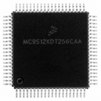
MC9S12XDT256CAA Freescale Semiconductor, MC9S12XDT256CAA Datasheet - Page 65

MC9S12XDT256CAA
Manufacturer Part Number
MC9S12XDT256CAA
Description
IC MCU 256K FLASH 80-QFP
Manufacturer
Freescale Semiconductor
Series
HCS12r
Datasheet
1.MC9S12XD64CAA.pdf
(1348 pages)
Specifications of MC9S12XDT256CAA
Core Processor
HCS12X
Core Size
16-Bit
Speed
80MHz
Connectivity
CAN, EBI/EMI, I²C, IrDA, LIN, SCI, SPI
Peripherals
LVD, POR, PWM, WDT
Number Of I /o
59
Program Memory Size
256KB (256K x 8)
Program Memory Type
FLASH
Eeprom Size
4K x 8
Ram Size
16K x 8
Voltage - Supply (vcc/vdd)
2.35 V ~ 5.5 V
Data Converters
A/D 8x10b
Oscillator Type
External
Operating Temperature
-40°C ~ 85°C
Package / Case
80-QFP
Processor Series
S12XD
Core
HCS12
Data Bus Width
16 bit
Data Ram Size
16 KB
Interface Type
CAN/I2C/SCI/SPI
Maximum Clock Frequency
40 MHz
Number Of Programmable I/os
59
Number Of Timers
12
Maximum Operating Temperature
+ 85 C
Mounting Style
SMD/SMT
3rd Party Development Tools
EWHCS12
Development Tools By Supplier
EVB9S12XDP512E
Minimum Operating Temperature
- 40 C
On-chip Adc
8-ch x 10-bit
Lead Free Status / RoHS Status
Lead free / RoHS Compliant
Available stocks
Company
Part Number
Manufacturer
Quantity
Price
Company:
Part Number:
MC9S12XDT256CAA
Manufacturer:
Freescale Semiconductor
Quantity:
10 000
Company:
Part Number:
MC9S12XDT256CAAR
Manufacturer:
Freescale Semiconductor
Quantity:
10 000
- Current page: 65 of 1348
- Download datasheet (8Mb)
1.2.3.62
PS5 is a general-purpose input or output pin. It can be configured as master output (during master mode)
or slave input pin (during slave mode) MOSI of the serial peripheral interface 0 (SPI0).
1.2.3.63
PS4 is a general-purpose input or output pin. It can be configured as master input (during master mode) or
slave output pin (during slave mode) MOSI of the serial peripheral interface 0 (SPI0).
1.2.3.64
PS3 is a general-purpose input or output pin. It can be configured as the transmit pin TXD of serial
communication interface 1 (SCI1).
1.2.3.65
PS2 is a general-purpose input or output pin. It can be configured as the receive pin RXD of serial
communication interface 1 (SCI1).
1.2.3.66
PS1 is a general-purpose input or output pin. It can be configured as the transmit pin TXD of serial
communication interface 0 (SCI0).
1.2.3.67
PS0 is a general-purpose input or output pin. It can be configured as the receive pin RXD of serial
communication interface 0 (SCI0).
1.2.3.68
PT[7:0] are general-purpose input or output pins. They can be configured as input capture or output
compare pins IOC[7:0] of the enhanced capture timer (ECT).
1.2.4
MC9S12XDP512RMV2 power and ground pins are described below.
1.2.4.1
External power and ground for I/O drivers. Because fast signal transitions place high, short-duration
current demands on the power supply, use bypass capacitors with high-frequency characteristics and place
them as close to the MCU as possible. Bypass requirements depend on how heavily the MCU pins are
loaded.
Freescale Semiconductor
Power Supply Pins
PS5 / MOSI0 — Port S I/O Pin 5
PS4 / MISO0 — Port S I/O Pin 4
PS3 / TXD1 — Port S I/O Pin 3
PS2 / RXD1 — Port S I/O Pin 2
PS1 / TXD0 — Port S I/O Pin 1
PS0 / RXD0 — Port S I/O Pin 0
PT[7:0] / IOC[7:0] — Port T I/O Pins [7:0]
V
All V
DDX1
SS
, V
pins must be connected together in the application.
DDX2
, V
SSX1
MC9S12XDP512 Data Sheet, Rev. 2.21
,V
SSX2
— Power and Ground Pins for I/O Drivers
NOTE
Chapter 1 Device Overview MC9S12XD-Family
65
Related parts for MC9S12XDT256CAA
Image
Part Number
Description
Manufacturer
Datasheet
Request
R

Part Number:
Description:
16-BIT MICROPROCESSOR FAMILY
Manufacturer:
FREESCALE [Freescale Semiconductor, Inc]
Datasheet:
Part Number:
Description:
Manufacturer:
Freescale Semiconductor, Inc
Datasheet:
Part Number:
Description:
Manufacturer:
Freescale Semiconductor, Inc
Datasheet:
Part Number:
Description:
Manufacturer:
Freescale Semiconductor, Inc
Datasheet:
Part Number:
Description:
Manufacturer:
Freescale Semiconductor, Inc
Datasheet:
Part Number:
Description:
Manufacturer:
Freescale Semiconductor, Inc
Datasheet:
Part Number:
Description:
Manufacturer:
Freescale Semiconductor, Inc
Datasheet:
Part Number:
Description:
Manufacturer:
Freescale Semiconductor, Inc
Datasheet:
Part Number:
Description:
Manufacturer:
Freescale Semiconductor, Inc
Datasheet:
Part Number:
Description:
Manufacturer:
Freescale Semiconductor, Inc
Datasheet:
Part Number:
Description:
Manufacturer:
Freescale Semiconductor, Inc
Datasheet:
Part Number:
Description:
Manufacturer:
Freescale Semiconductor, Inc
Datasheet:
Part Number:
Description:
Manufacturer:
Freescale Semiconductor, Inc
Datasheet:
Part Number:
Description:
Manufacturer:
Freescale Semiconductor, Inc
Datasheet:
Part Number:
Description:
Manufacturer:
Freescale Semiconductor, Inc
Datasheet:


