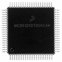
MC9S12XDT256CAA Freescale Semiconductor, MC9S12XDT256CAA Datasheet - Page 652

MC9S12XDT256CAA
Manufacturer Part Number
MC9S12XDT256CAA
Description
IC MCU 256K FLASH 80-QFP
Manufacturer
Freescale Semiconductor
Series
HCS12r
Datasheet
1.MC9S12XD64CAA.pdf
(1348 pages)
Specifications of MC9S12XDT256CAA
Core Processor
HCS12X
Core Size
16-Bit
Speed
80MHz
Connectivity
CAN, EBI/EMI, I²C, IrDA, LIN, SCI, SPI
Peripherals
LVD, POR, PWM, WDT
Number Of I /o
59
Program Memory Size
256KB (256K x 8)
Program Memory Type
FLASH
Eeprom Size
4K x 8
Ram Size
16K x 8
Voltage - Supply (vcc/vdd)
2.35 V ~ 5.5 V
Data Converters
A/D 8x10b
Oscillator Type
External
Operating Temperature
-40°C ~ 85°C
Package / Case
80-QFP
Processor Series
S12XD
Core
HCS12
Data Bus Width
16 bit
Data Ram Size
16 KB
Interface Type
CAN/I2C/SCI/SPI
Maximum Clock Frequency
40 MHz
Number Of Programmable I/os
59
Number Of Timers
12
Maximum Operating Temperature
+ 85 C
Mounting Style
SMD/SMT
3rd Party Development Tools
EWHCS12
Development Tools By Supplier
EVB9S12XDP512E
Minimum Operating Temperature
- 40 C
On-chip Adc
8-ch x 10-bit
Lead Free Status / RoHS Status
Lead free / RoHS Compliant
Available stocks
Company
Part Number
Manufacturer
Quantity
Price
Company:
Part Number:
MC9S12XDT256CAA
Manufacturer:
Freescale Semiconductor
Quantity:
10 000
Company:
Part Number:
MC9S12XDT256CAAR
Manufacturer:
Freescale Semiconductor
Quantity:
10 000
- Current page: 652 of 1348
- Download datasheet (8Mb)
Chapter 18 Memory Mapping Control (S12XMMCV3)
18.1.1
18.1.2
The main features of this block are:
652
•
•
Unimplemented areas
Mis-aligned address
single-chip modes
Paging capability to support a global 8 Mbytes memory address space
Bus arbitration between the masters CPU, BDM and XGATE
external resource
expanded modes
emulation modes
Aligned address
External Space
global address
normal modes
special modes
Logic level “1”
Logic level “0”
local address
Bus Clock
Terminology
Features
MCU
NVM
word
PRR
PRU
byte
NS
SS
NX
ES
EX
ST
0x
x
Voltage that corresponds to Boolean true state
Voltage that corresponds to Boolean false state
Represents hexadecimal number
Represents logic level ’don’t care’
8-bit data
16-bit data
based on the 64 KBytes Memory Space (16-bit address)
based on the 8 MBytes Memory Space (23-bit address)
Address on even boundary
Address on odd boundary
System Clock. Refer to CRG Block Guide.
Normal Expanded Mode
Emulation Single-Chip Mode
Emulation Expanded Mode
Special Test Mode
Normal Single-Chip Mode
Special Single-Chip Mode
Emulation Single-Chip Mode
Emulation Expanded Mode
Normal Single-Chip Mode
Normal Expanded Mode
Special Single-Chip Mode
Special Test Mode
Normal Single-Chip Mode
Special Single-Chip Mode
Normal Expanded Mode
Emulation Single-Chip Mode
Emulation Expanded Mode
Special Test Mode
Areas which are accessible by the pages (RPAGE,PPAGE,EPAGE) and not implemented
Area which is accessible in the global address range 14_0000 to 3F_FFFF
Resources (Emulator, Application) connected to the MCU via the external bus on
expanded modes (Unimplemented areas and External Space)
Port Replacement Registers
Port Replacement Unit located on the emulator side
MicroController Unit
Non-volatile Memory; Flash EEPROM or ROM
Table 18-1. Acronyms and Abbreviations
MC9S12XDP512 Data Sheet, Rev. 2.21
Freescale Semiconductor
Related parts for MC9S12XDT256CAA
Image
Part Number
Description
Manufacturer
Datasheet
Request
R

Part Number:
Description:
16-BIT MICROPROCESSOR FAMILY
Manufacturer:
FREESCALE [Freescale Semiconductor, Inc]
Datasheet:
Part Number:
Description:
Manufacturer:
Freescale Semiconductor, Inc
Datasheet:
Part Number:
Description:
Manufacturer:
Freescale Semiconductor, Inc
Datasheet:
Part Number:
Description:
Manufacturer:
Freescale Semiconductor, Inc
Datasheet:
Part Number:
Description:
Manufacturer:
Freescale Semiconductor, Inc
Datasheet:
Part Number:
Description:
Manufacturer:
Freescale Semiconductor, Inc
Datasheet:
Part Number:
Description:
Manufacturer:
Freescale Semiconductor, Inc
Datasheet:
Part Number:
Description:
Manufacturer:
Freescale Semiconductor, Inc
Datasheet:
Part Number:
Description:
Manufacturer:
Freescale Semiconductor, Inc
Datasheet:
Part Number:
Description:
Manufacturer:
Freescale Semiconductor, Inc
Datasheet:
Part Number:
Description:
Manufacturer:
Freescale Semiconductor, Inc
Datasheet:
Part Number:
Description:
Manufacturer:
Freescale Semiconductor, Inc
Datasheet:
Part Number:
Description:
Manufacturer:
Freescale Semiconductor, Inc
Datasheet:
Part Number:
Description:
Manufacturer:
Freescale Semiconductor, Inc
Datasheet:
Part Number:
Description:
Manufacturer:
Freescale Semiconductor, Inc
Datasheet:


