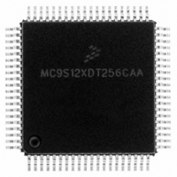
MC9S12XDT256CAA Freescale Semiconductor, MC9S12XDT256CAA Datasheet - Page 664

MC9S12XDT256CAA
Manufacturer Part Number
MC9S12XDT256CAA
Description
IC MCU 256K FLASH 80-QFP
Manufacturer
Freescale Semiconductor
Series
HCS12r
Datasheet
1.MC9S12XD64CAA.pdf
(1348 pages)
Specifications of MC9S12XDT256CAA
Core Processor
HCS12X
Core Size
16-Bit
Speed
80MHz
Connectivity
CAN, EBI/EMI, I²C, IrDA, LIN, SCI, SPI
Peripherals
LVD, POR, PWM, WDT
Number Of I /o
59
Program Memory Size
256KB (256K x 8)
Program Memory Type
FLASH
Eeprom Size
4K x 8
Ram Size
16K x 8
Voltage - Supply (vcc/vdd)
2.35 V ~ 5.5 V
Data Converters
A/D 8x10b
Oscillator Type
External
Operating Temperature
-40°C ~ 85°C
Package / Case
80-QFP
Processor Series
S12XD
Core
HCS12
Data Bus Width
16 bit
Data Ram Size
16 KB
Interface Type
CAN/I2C/SCI/SPI
Maximum Clock Frequency
40 MHz
Number Of Programmable I/os
59
Number Of Timers
12
Maximum Operating Temperature
+ 85 C
Mounting Style
SMD/SMT
3rd Party Development Tools
EWHCS12
Development Tools By Supplier
EVB9S12XDP512E
Minimum Operating Temperature
- 40 C
On-chip Adc
8-ch x 10-bit
Lead Free Status / RoHS Status
Lead free / RoHS Compliant
Available stocks
Company
Part Number
Manufacturer
Quantity
Price
Company:
Part Number:
MC9S12XDT256CAA
Manufacturer:
Freescale Semiconductor
Quantity:
10 000
Company:
Part Number:
MC9S12XDT256CAAR
Manufacturer:
Freescale Semiconductor
Quantity:
10 000
- Current page: 664 of 1348
- Download datasheet (8Mb)
Chapter 18 Memory Mapping Control (S12XMMCV3)
18.3.2.6
Read: Anytime
Write: Anytime
These eight index bits are used to page 4 KByte blocks into the RAM page window located in the local
(CPU or BDM) memory map from address 0x1000 to address 0x1FFF (see
accessing up to 1022 Kbytes of RAM (in the Global map) within the 64 KByte Local map. The RAM page
index register is effectively used to construct paged RAM addresses in the Local map
664
Address: 0x0016
Reset
W
R
1
2
Internal Flash means Flash resources inside the MCU are read/written.
Emulation memory means resources inside the emulator are read/written (PRU registers, flash
replacement, RAM, EEPROM and register space are always considered internal).
External application means resources residing outside the MCU are read/written.
The external access stretch mechanism is part of the EBI module (refer to EBI Block Guide for details).
Emulation Single Chip
Emulation Expanded
RP7
Special Single Chip
Normal Single Chip
RAM Page Index Register (RPAGE)
Normal Expanded
1
7
XGATE write access to this register during an CPU access which makes use
of this register could lead to unexpected results.
Chip Modes
Special Test
Table 18-11. Data Sources when CPU or BDM is Accessing Flash Area
RP6
1
6
Figure 18-11. RAM Page Index Register (RPAGE)
MC9S12XDP512 Data Sheet, Rev. 2.21
RP5
ROMON
1
5
X
X
X
0
1
0
1
1
0
1
CAUTION
RP4
EROMON
1
4
X
X
X
X
X
X
0
1
0
1
RP3
1
3
External Application
External Application
External Application
Emulation Memory
Emulation Memory
DATA SOURCE
Internal Flash
Internal Flash
Internal Flash
Internal Flash
Internal Flash
RP2
1
2
Figure
1
18-12). This supports
Freescale Semiconductor
RP1
format.
0
1
Stretch
N
N
N
N
N
Y
Y
2
RP0
1
0
Related parts for MC9S12XDT256CAA
Image
Part Number
Description
Manufacturer
Datasheet
Request
R

Part Number:
Description:
16-BIT MICROPROCESSOR FAMILY
Manufacturer:
FREESCALE [Freescale Semiconductor, Inc]
Datasheet:
Part Number:
Description:
Manufacturer:
Freescale Semiconductor, Inc
Datasheet:
Part Number:
Description:
Manufacturer:
Freescale Semiconductor, Inc
Datasheet:
Part Number:
Description:
Manufacturer:
Freescale Semiconductor, Inc
Datasheet:
Part Number:
Description:
Manufacturer:
Freescale Semiconductor, Inc
Datasheet:
Part Number:
Description:
Manufacturer:
Freescale Semiconductor, Inc
Datasheet:
Part Number:
Description:
Manufacturer:
Freescale Semiconductor, Inc
Datasheet:
Part Number:
Description:
Manufacturer:
Freescale Semiconductor, Inc
Datasheet:
Part Number:
Description:
Manufacturer:
Freescale Semiconductor, Inc
Datasheet:
Part Number:
Description:
Manufacturer:
Freescale Semiconductor, Inc
Datasheet:
Part Number:
Description:
Manufacturer:
Freescale Semiconductor, Inc
Datasheet:
Part Number:
Description:
Manufacturer:
Freescale Semiconductor, Inc
Datasheet:
Part Number:
Description:
Manufacturer:
Freescale Semiconductor, Inc
Datasheet:
Part Number:
Description:
Manufacturer:
Freescale Semiconductor, Inc
Datasheet:
Part Number:
Description:
Manufacturer:
Freescale Semiconductor, Inc
Datasheet:


