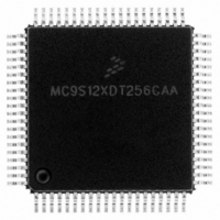
MC9S12XDT256CAA Freescale Semiconductor, MC9S12XDT256CAA Datasheet - Page 675

MC9S12XDT256CAA
Manufacturer Part Number
MC9S12XDT256CAA
Description
IC MCU 256K FLASH 80-QFP
Manufacturer
Freescale Semiconductor
Series
HCS12r
Datasheet
1.MC9S12XD64CAA.pdf
(1348 pages)
Specifications of MC9S12XDT256CAA
Core Processor
HCS12X
Core Size
16-Bit
Speed
80MHz
Connectivity
CAN, EBI/EMI, I²C, IrDA, LIN, SCI, SPI
Peripherals
LVD, POR, PWM, WDT
Number Of I /o
59
Program Memory Size
256KB (256K x 8)
Program Memory Type
FLASH
Eeprom Size
4K x 8
Ram Size
16K x 8
Voltage - Supply (vcc/vdd)
2.35 V ~ 5.5 V
Data Converters
A/D 8x10b
Oscillator Type
External
Operating Temperature
-40°C ~ 85°C
Package / Case
80-QFP
Processor Series
S12XD
Core
HCS12
Data Bus Width
16 bit
Data Ram Size
16 KB
Interface Type
CAN/I2C/SCI/SPI
Maximum Clock Frequency
40 MHz
Number Of Programmable I/os
59
Number Of Timers
12
Maximum Operating Temperature
+ 85 C
Mounting Style
SMD/SMT
3rd Party Development Tools
EWHCS12
Development Tools By Supplier
EVB9S12XDP512E
Minimum Operating Temperature
- 40 C
On-chip Adc
8-ch x 10-bit
Lead Free Status / RoHS Status
Lead free / RoHS Compliant
Available stocks
Company
Part Number
Manufacturer
Quantity
Price
Company:
Part Number:
MC9S12XDT256CAA
Manufacturer:
Freescale Semiconductor
Quantity:
10 000
Company:
Part Number:
MC9S12XDT256CAAR
Manufacturer:
Freescale Semiconductor
Quantity:
10 000
- Current page: 675 of 1348
- Download datasheet (8Mb)
Chapter 18 Memory Mapping Control (S12XMMCV3)
Expansion of the BDM Local Address Map
PPAGE, RPAGE, and EPAGE registers are also used for the expansion of the BDM local address to the
global address. These registers can be read and written by the BDM.
The BDM expansion scheme is the same as the CPU expansion scheme.
18.4.2.2
Global Addresses Based on the Global Page
CPU Global Addresses Based on the Global Page
The seven global page index bits allow access to the full 8 Mbyte address map that can be accessed with
23 address bits. This provides an alternative way to access all of the various pages of FLASH, RAM and
EEPROM as well as additional external memory.
The GPAGE Register is used only when the CPU is executing a global instruction (see
Section 18.3.2.3,
“Global Page Index Register
(GPAGE)). The generated global address is the result of concatenation of the
CPU local address [15:0] with the GPAGE register [22:16] (see
Figure
18-7).
BDM Global Addresses Based on the Global Page
The seven BDMGPR Global Page index bits allow access to the full 8 Mbyte address map that can be
accessed with 23 address bits. This provides an alternative way to access all of the various pages of
FLASH, RAM and EEPROM as well as additional external memory.
The BDM global page index register (BDMGPR) is used only in the case the CPU is executing a firmware
command which uses a global instruction (like GLDD, GSTD) or by a BDM hardware command (like
WRITE_W, WRITE_BYTE, READ_W, READ_BYTE). See the BDM Block Guide for further details.
The generated global address is a result of concatenation of the BDM local address with the BDMGPR
register [22:16] in the case of a hardware command or concatenation of the CPU local address and the
BDMGPR register [22:16] in the case of a firmware command (see
Figure
18-22).
MC9S12XDP512 Data Sheet, Rev. 2.21
Freescale Semiconductor
675
Related parts for MC9S12XDT256CAA
Image
Part Number
Description
Manufacturer
Datasheet
Request
R

Part Number:
Description:
16-BIT MICROPROCESSOR FAMILY
Manufacturer:
FREESCALE [Freescale Semiconductor, Inc]
Datasheet:
Part Number:
Description:
Manufacturer:
Freescale Semiconductor, Inc
Datasheet:
Part Number:
Description:
Manufacturer:
Freescale Semiconductor, Inc
Datasheet:
Part Number:
Description:
Manufacturer:
Freescale Semiconductor, Inc
Datasheet:
Part Number:
Description:
Manufacturer:
Freescale Semiconductor, Inc
Datasheet:
Part Number:
Description:
Manufacturer:
Freescale Semiconductor, Inc
Datasheet:
Part Number:
Description:
Manufacturer:
Freescale Semiconductor, Inc
Datasheet:
Part Number:
Description:
Manufacturer:
Freescale Semiconductor, Inc
Datasheet:
Part Number:
Description:
Manufacturer:
Freescale Semiconductor, Inc
Datasheet:
Part Number:
Description:
Manufacturer:
Freescale Semiconductor, Inc
Datasheet:
Part Number:
Description:
Manufacturer:
Freescale Semiconductor, Inc
Datasheet:
Part Number:
Description:
Manufacturer:
Freescale Semiconductor, Inc
Datasheet:
Part Number:
Description:
Manufacturer:
Freescale Semiconductor, Inc
Datasheet:
Part Number:
Description:
Manufacturer:
Freescale Semiconductor, Inc
Datasheet:
Part Number:
Description:
Manufacturer:
Freescale Semiconductor, Inc
Datasheet:


