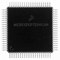
MC9S12XDT256CAA Freescale Semiconductor, MC9S12XDT256CAA Datasheet - Page 760

MC9S12XDT256CAA
Manufacturer Part Number
MC9S12XDT256CAA
Description
IC MCU 256K FLASH 80-QFP
Manufacturer
Freescale Semiconductor
Series
HCS12r
Datasheet
1.MC9S12XD64CAA.pdf
(1348 pages)
Specifications of MC9S12XDT256CAA
Core Processor
HCS12X
Core Size
16-Bit
Speed
80MHz
Connectivity
CAN, EBI/EMI, I²C, IrDA, LIN, SCI, SPI
Peripherals
LVD, POR, PWM, WDT
Number Of I /o
59
Program Memory Size
256KB (256K x 8)
Program Memory Type
FLASH
Eeprom Size
4K x 8
Ram Size
16K x 8
Voltage - Supply (vcc/vdd)
2.35 V ~ 5.5 V
Data Converters
A/D 8x10b
Oscillator Type
External
Operating Temperature
-40°C ~ 85°C
Package / Case
80-QFP
Processor Series
S12XD
Core
HCS12
Data Bus Width
16 bit
Data Ram Size
16 KB
Interface Type
CAN/I2C/SCI/SPI
Maximum Clock Frequency
40 MHz
Number Of Programmable I/os
59
Number Of Timers
12
Maximum Operating Temperature
+ 85 C
Mounting Style
SMD/SMT
3rd Party Development Tools
EWHCS12
Development Tools By Supplier
EVB9S12XDP512E
Minimum Operating Temperature
- 40 C
On-chip Adc
8-ch x 10-bit
Lead Free Status / RoHS Status
Lead free / RoHS Compliant
Available stocks
Company
Part Number
Manufacturer
Quantity
Price
Company:
Part Number:
MC9S12XDT256CAA
Manufacturer:
Freescale Semiconductor
Quantity:
10 000
Company:
Part Number:
MC9S12XDT256CAAR
Manufacturer:
Freescale Semiconductor
Quantity:
10 000
- Current page: 760 of 1348
- Download datasheet (8Mb)
Chapter 20 S12X Debug (S12XDBGV3) Module
20.3.2.7.4
Read: Anytime
Write: Never
DBGMFR is visible at 0x0027 only with COMRV[1:0] = 11. It features four flag bits each mapped directly
to a channel. Should a match occur on the channel during the debug session, then the corresponding flag
is set and remains set until the next time the module is armed by writing to the ARM bit. Thus the contents
are retained after a debug session for evaluation purposes. These flags cannot be cleared by software, they
are cleared only when arming the module. A set flag does not inhibit the setting of other flags. Once a flag
is set, further triggers on the same channel have no affect.
20.3.2.8
Each comparator has a bank of registers that are visible through an 8-byte window in the S12XDBG
module register address map. Comparators A and C consist of 8 register bytes (3 address bus compare
registers, two data bus compare registers, two data bus mask registers and a control register).
Comparators B and D consist of four register bytes (three address bus compare registers and a control
register).
Each set of comparator registers is accessible in the same 8-byte window of the register address map and
can be accessed using the COMRV bits in the DBGC1 register. If the Comparators B or D are accessed
through the 8-byte window, then only the address and control bytes are visible, the 4 bytes associated with
data bus and data bus masking read as zero and cannot be written. Furthermore the control registers for
comparators B and D differ from those of comparators A and C.
762
Address: 0x0027
0x002A
0x002B
0x002C
0x002D
0x002E
0x0028
0x0029
0x002F
Reset
W
R
Comparator Register Descriptions
0
0
7
Debug Match Flag Register (DBGMFR)
DATA HIGH COMPARATOR
DATA LOW COMPARATOR
= Unimplemented or Reserved
ADDRESS MEDIUM
DATA HIGH MASK
DATA LOW MASK
ADDRESS HIGH
ADDRESS LOW
0
0
6
Figure 20-12. Debug Match Flag Register (DBGMFR)
CONTROL
Table 20-26. Comparator Register Layout
MC9S12XDP512 Data Sheet, Rev. 2.21
0
0
5
0
0
4
Read/Write
Read/Write
Read/Write
Read/Write
Read/Write
Read/Write
Read/Write
Read/Write
MC3
0
3
MC2
0
2
Comparator A and C only
Comparator A and C only
Comparator A and C only
Comparator A and C only
Freescale Semiconductor
MC1
—
—
—
—
0
1
MC0
0
0
Related parts for MC9S12XDT256CAA
Image
Part Number
Description
Manufacturer
Datasheet
Request
R

Part Number:
Description:
16-BIT MICROPROCESSOR FAMILY
Manufacturer:
FREESCALE [Freescale Semiconductor, Inc]
Datasheet:
Part Number:
Description:
Manufacturer:
Freescale Semiconductor, Inc
Datasheet:
Part Number:
Description:
Manufacturer:
Freescale Semiconductor, Inc
Datasheet:
Part Number:
Description:
Manufacturer:
Freescale Semiconductor, Inc
Datasheet:
Part Number:
Description:
Manufacturer:
Freescale Semiconductor, Inc
Datasheet:
Part Number:
Description:
Manufacturer:
Freescale Semiconductor, Inc
Datasheet:
Part Number:
Description:
Manufacturer:
Freescale Semiconductor, Inc
Datasheet:
Part Number:
Description:
Manufacturer:
Freescale Semiconductor, Inc
Datasheet:
Part Number:
Description:
Manufacturer:
Freescale Semiconductor, Inc
Datasheet:
Part Number:
Description:
Manufacturer:
Freescale Semiconductor, Inc
Datasheet:
Part Number:
Description:
Manufacturer:
Freescale Semiconductor, Inc
Datasheet:
Part Number:
Description:
Manufacturer:
Freescale Semiconductor, Inc
Datasheet:
Part Number:
Description:
Manufacturer:
Freescale Semiconductor, Inc
Datasheet:
Part Number:
Description:
Manufacturer:
Freescale Semiconductor, Inc
Datasheet:
Part Number:
Description:
Manufacturer:
Freescale Semiconductor, Inc
Datasheet:


