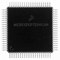
MC9S12XDT256CAA Freescale Semiconductor, MC9S12XDT256CAA Datasheet - Page 957

MC9S12XDT256CAA
Manufacturer Part Number
MC9S12XDT256CAA
Description
IC MCU 256K FLASH 80-QFP
Manufacturer
Freescale Semiconductor
Series
HCS12r
Datasheet
1.MC9S12XD64CAA.pdf
(1348 pages)
Specifications of MC9S12XDT256CAA
Core Processor
HCS12X
Core Size
16-Bit
Speed
80MHz
Connectivity
CAN, EBI/EMI, I²C, IrDA, LIN, SCI, SPI
Peripherals
LVD, POR, PWM, WDT
Number Of I /o
59
Program Memory Size
256KB (256K x 8)
Program Memory Type
FLASH
Eeprom Size
4K x 8
Ram Size
16K x 8
Voltage - Supply (vcc/vdd)
2.35 V ~ 5.5 V
Data Converters
A/D 8x10b
Oscillator Type
External
Operating Temperature
-40°C ~ 85°C
Package / Case
80-QFP
Processor Series
S12XD
Core
HCS12
Data Bus Width
16 bit
Data Ram Size
16 KB
Interface Type
CAN/I2C/SCI/SPI
Maximum Clock Frequency
40 MHz
Number Of Programmable I/os
59
Number Of Timers
12
Maximum Operating Temperature
+ 85 C
Mounting Style
SMD/SMT
3rd Party Development Tools
EWHCS12
Development Tools By Supplier
EVB9S12XDP512E
Minimum Operating Temperature
- 40 C
On-chip Adc
8-ch x 10-bit
Lead Free Status / RoHS Status
Lead free / RoHS Compliant
Available stocks
Company
Part Number
Manufacturer
Quantity
Price
Company:
Part Number:
MC9S12XDT256CAA
Manufacturer:
Freescale Semiconductor
Quantity:
10 000
Company:
Part Number:
MC9S12XDT256CAAR
Manufacturer:
Freescale Semiconductor
Quantity:
10 000
- Current page: 957 of 1348
- Download datasheet (8Mb)
DDR0AD1[23:16]
Reset
Reset
23.0.5.67 Port AD1 Data Register 1 (PT1AD1)
Read: Anytime.
Write: Anytime.
This register is associated with AD1 pins PAD[15:8]. These pins can also be used as general
purpose I/O.
If the data direction bits of the associated I/O pins are set to 1, a read returns the value of the port
register, otherwise the value at the pins is read.
23.0.5.68 Port AD1 Data Direction Register 0 (DDR0AD1)
Read: Anytime.
Write: Anytime.
This register configures pin PAD[23:16] as either input or output.
Field
W
W
R
R
7–0
DDR0AD123 DDR0AD122 DDR0AD121 DDR0AD120 DDR0AD119 DDR0AD118 DDR0AD117 DDR0AD116
PT1AD115
7
0
7
0
Data Direction Port AD1 Register 0
0 Associated pin is configured as input.
1 Associated pin is configured as output.
Note: Due to internal synchronization circuits, it can take up to 2 bus clock cycles until the correct value is
Note: To use the digital input function on Port AD1 the ATD1 digital input enable register (ATD1DIEN0) has
PT1AD114
read on PTAD10 register, when changing the DDR0AD1 register.
to be set to logic level “1”.
Figure 23-70. Port AD1 Data Direction Register 0 (DDR0AD1)
0
0
6
6
Figure 23-69. Port AD1 Data Register 1 (PT1AD1)
Table 23-61. DDR0AD1 Field Descriptions
PT1AD113
5
0
5
0
PT1AD112
0
0
4
4
Description
PT1AD111
3
0
3
0
PT1AD110
0
0
2
2
PT1AD19
1
0
1
0
PT1AD18
0
0
0
0
Related parts for MC9S12XDT256CAA
Image
Part Number
Description
Manufacturer
Datasheet
Request
R

Part Number:
Description:
16-BIT MICROPROCESSOR FAMILY
Manufacturer:
FREESCALE [Freescale Semiconductor, Inc]
Datasheet:
Part Number:
Description:
Manufacturer:
Freescale Semiconductor, Inc
Datasheet:
Part Number:
Description:
Manufacturer:
Freescale Semiconductor, Inc
Datasheet:
Part Number:
Description:
Manufacturer:
Freescale Semiconductor, Inc
Datasheet:
Part Number:
Description:
Manufacturer:
Freescale Semiconductor, Inc
Datasheet:
Part Number:
Description:
Manufacturer:
Freescale Semiconductor, Inc
Datasheet:
Part Number:
Description:
Manufacturer:
Freescale Semiconductor, Inc
Datasheet:
Part Number:
Description:
Manufacturer:
Freescale Semiconductor, Inc
Datasheet:
Part Number:
Description:
Manufacturer:
Freescale Semiconductor, Inc
Datasheet:
Part Number:
Description:
Manufacturer:
Freescale Semiconductor, Inc
Datasheet:
Part Number:
Description:
Manufacturer:
Freescale Semiconductor, Inc
Datasheet:
Part Number:
Description:
Manufacturer:
Freescale Semiconductor, Inc
Datasheet:
Part Number:
Description:
Manufacturer:
Freescale Semiconductor, Inc
Datasheet:
Part Number:
Description:
Manufacturer:
Freescale Semiconductor, Inc
Datasheet:
Part Number:
Description:
Manufacturer:
Freescale Semiconductor, Inc
Datasheet:


