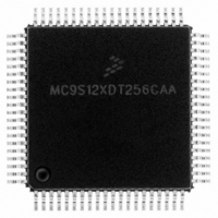
MC9S12XDT256CAA Freescale Semiconductor, MC9S12XDT256CAA Datasheet - Page 99

MC9S12XDT256CAA
Manufacturer Part Number
MC9S12XDT256CAA
Description
IC MCU 256K FLASH 80-QFP
Manufacturer
Freescale Semiconductor
Series
HCS12r
Datasheet
1.MC9S12XD64CAA.pdf
(1348 pages)
Specifications of MC9S12XDT256CAA
Core Processor
HCS12X
Core Size
16-Bit
Speed
80MHz
Connectivity
CAN, EBI/EMI, I²C, IrDA, LIN, SCI, SPI
Peripherals
LVD, POR, PWM, WDT
Number Of I /o
59
Program Memory Size
256KB (256K x 8)
Program Memory Type
FLASH
Eeprom Size
4K x 8
Ram Size
16K x 8
Voltage - Supply (vcc/vdd)
2.35 V ~ 5.5 V
Data Converters
A/D 8x10b
Oscillator Type
External
Operating Temperature
-40°C ~ 85°C
Package / Case
80-QFP
Processor Series
S12XD
Core
HCS12
Data Bus Width
16 bit
Data Ram Size
16 KB
Interface Type
CAN/I2C/SCI/SPI
Maximum Clock Frequency
40 MHz
Number Of Programmable I/os
59
Number Of Timers
12
Maximum Operating Temperature
+ 85 C
Mounting Style
SMD/SMT
3rd Party Development Tools
EWHCS12
Development Tools By Supplier
EVB9S12XDP512E
Minimum Operating Temperature
- 40 C
On-chip Adc
8-ch x 10-bit
Lead Free Status / RoHS Status
Lead free / RoHS Compliant
Available stocks
Company
Part Number
Manufacturer
Quantity
Price
Company:
Part Number:
MC9S12XDT256CAA
Manufacturer:
Freescale Semiconductor
Quantity:
10 000
Company:
Part Number:
MC9S12XDT256CAAR
Manufacturer:
Freescale Semiconductor
Quantity:
10 000
- Current page: 99 of 1348
- Download datasheet (8Mb)
2.4.1.1.1
The oscillator output clock signal (OSCCLK) is fed through the reference programmable divider and is
divided in a range of 1 to 64 (REFDV + 1) to output the REFERENCE clock. The VCO output clock,
(PLLCLK) is fed back through the programmable loop divider and is divided in a range of 2 to 128 in
increments of [2 x (SYNR + 1)] to output the FEEDBACK clock.
The phase detector then compares the FEEDBACK clock, with the REFERENCE clock. Correction pulses
are generated based on the phase difference between the two signals. The loop filter then slightly alters the
DC voltage on the external filter capacitor connected to XFC pin, based on the width and direction of the
correction pulse. The filter can make fast or slow corrections depending on its mode, as described in the
next subsection. The values of the external filter network and the reference frequency determine the speed
of the corrections and the stability of the PLL.
The minimum VCO frequency is reached with the XFC pin forced to V
frequency.
2.4.1.1.2
The lock detector compares the frequencies of the FEEDBACK clock, and the REFERENCE clock.
Therefore, the speed of the lock detector is directly proportional to the final reference frequency. The
circuit determines the mode of the PLL and the lock condition based on this comparison.
The PLL filter can be manually or automatically configured into one of two possible operating modes:
The PLL can change the bandwidth or operational mode of the loop filter manually or automatically.
In automatic bandwidth control mode (AUTO = 1), the lock detector automatically switches between
acquisition and tracking modes. Automatic bandwidth control mode also is used to determine when the
PLL clock (PLLCLK) is safe to use as the source for the system and core clocks. If PLL LOCK interrupt
requests are enabled, the software can wait for an interrupt request and then check the LOCK bit. If
interrupt requests are disabled, software can poll the LOCK bit continuously (during PLL start-up, usually)
or at periodic intervals. In either case, only when the LOCK bit is set, is the PLLCLK clock safe to use as
the source for the system and core clocks. If the PLL is selected as the source for the system and core clocks
and the LOCK bit is clear, the PLL has suffered a severe noise hit and the software must take appropriate
action, depending on the application.
Freescale Semiconductor
•
•
Acquisition mode
In acquisition mode, the filter can make large frequency corrections to the VCO. This mode is used
at PLL start-up or when the PLL has suffered a severe noise hit and the VCO frequency is far off
the desired frequency. When in acquisition mode, the TRACK status bit is cleared in the CRGFLG
register.
Tracking mode
In tracking mode, the filter makes only small corrections to the frequency of the VCO. PLL jitter
is much lower in tracking mode, but the response to noise is also slower. The PLL enters tracking
mode when the VCO frequency is nearly correct and the TRACK bit is set in the CRGFLG register.
PLL Operation
Acquisition and Tracking Modes
MC9S12XDP512 Data Sheet, Rev. 2.21
Chapter 2 Clocks and Reset Generator (S12CRGV6)
Figure
DDPLL
2-16.
. This is the self clock mode
99
Related parts for MC9S12XDT256CAA
Image
Part Number
Description
Manufacturer
Datasheet
Request
R

Part Number:
Description:
16-BIT MICROPROCESSOR FAMILY
Manufacturer:
FREESCALE [Freescale Semiconductor, Inc]
Datasheet:
Part Number:
Description:
Manufacturer:
Freescale Semiconductor, Inc
Datasheet:
Part Number:
Description:
Manufacturer:
Freescale Semiconductor, Inc
Datasheet:
Part Number:
Description:
Manufacturer:
Freescale Semiconductor, Inc
Datasheet:
Part Number:
Description:
Manufacturer:
Freescale Semiconductor, Inc
Datasheet:
Part Number:
Description:
Manufacturer:
Freescale Semiconductor, Inc
Datasheet:
Part Number:
Description:
Manufacturer:
Freescale Semiconductor, Inc
Datasheet:
Part Number:
Description:
Manufacturer:
Freescale Semiconductor, Inc
Datasheet:
Part Number:
Description:
Manufacturer:
Freescale Semiconductor, Inc
Datasheet:
Part Number:
Description:
Manufacturer:
Freescale Semiconductor, Inc
Datasheet:
Part Number:
Description:
Manufacturer:
Freescale Semiconductor, Inc
Datasheet:
Part Number:
Description:
Manufacturer:
Freescale Semiconductor, Inc
Datasheet:
Part Number:
Description:
Manufacturer:
Freescale Semiconductor, Inc
Datasheet:
Part Number:
Description:
Manufacturer:
Freescale Semiconductor, Inc
Datasheet:
Part Number:
Description:
Manufacturer:
Freescale Semiconductor, Inc
Datasheet:


