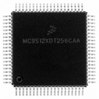
MC9S12XDT256CAA Freescale Semiconductor, MC9S12XDT256CAA Datasheet - Page 999

MC9S12XDT256CAA
Manufacturer Part Number
MC9S12XDT256CAA
Description
IC MCU 256K FLASH 80-QFP
Manufacturer
Freescale Semiconductor
Series
HCS12r
Datasheet
1.MC9S12XD64CAA.pdf
(1348 pages)
Specifications of MC9S12XDT256CAA
Core Processor
HCS12X
Core Size
16-Bit
Speed
80MHz
Connectivity
CAN, EBI/EMI, I²C, IrDA, LIN, SCI, SPI
Peripherals
LVD, POR, PWM, WDT
Number Of I /o
59
Program Memory Size
256KB (256K x 8)
Program Memory Type
FLASH
Eeprom Size
4K x 8
Ram Size
16K x 8
Voltage - Supply (vcc/vdd)
2.35 V ~ 5.5 V
Data Converters
A/D 8x10b
Oscillator Type
External
Operating Temperature
-40°C ~ 85°C
Package / Case
80-QFP
Processor Series
S12XD
Core
HCS12
Data Bus Width
16 bit
Data Ram Size
16 KB
Interface Type
CAN/I2C/SCI/SPI
Maximum Clock Frequency
40 MHz
Number Of Programmable I/os
59
Number Of Timers
12
Maximum Operating Temperature
+ 85 C
Mounting Style
SMD/SMT
3rd Party Development Tools
EWHCS12
Development Tools By Supplier
EVB9S12XDP512E
Minimum Operating Temperature
- 40 C
On-chip Adc
8-ch x 10-bit
Lead Free Status / RoHS Status
Lead free / RoHS Compliant
Available stocks
Company
Part Number
Manufacturer
Quantity
Price
Company:
Part Number:
MC9S12XDT256CAA
Manufacturer:
Freescale Semiconductor
Quantity:
10 000
Company:
Part Number:
MC9S12XDT256CAAR
Manufacturer:
Freescale Semiconductor
Quantity:
10 000
- Current page: 999 of 1348
- Download datasheet (8Mb)
PTIT[7:0]
Reset
PTT[7:0]
Reset
Field
24.0.5.14 Port T Input Register (PTIT)
1. These registers are reset to zero. Two bus clock cycles after reset release the register values are updated with the
Read: Anytime.
Write: Never, writes to this register have no effect.
Field
24.0.5.15 Port T Data Direction Register (DDRT)
Read: Anytime.
Write: Anytime.
This register configures each port T pin as either input or output.
The ECT forces the I/O state to be an output for each timer port associated with an enabled output
compare. In this case the data direction bits will not change.
7–0
7–0
W
associated pin values.
W
R
R
1
DDRT7
PTIT7
Port T — Port T bits 7–0 are associated with ECT channels IOC7–IOC0 (refer to ECT section). When not used
with the ECT, these pins can be used as general purpose I/O.
If the data direction bits of the associated I/O pins are set to logic level “1”, a read returns the value of the port
register, otherwise the buffered pin input state is read.
Port T Input — This register always reads back the buffered state of the associated pins. This can also be used
to detect overload or short circuit conditions on output pins.
—
7
7
0
= Unimplemented or Reserved
DDRT6
PTIT6
—
0
6
6
Figure 24-17. Port T Data Direction Register (DDRT)
Figure 24-16. Port T Input Register (PTIT)
Table 24-18. PTIT Field Descriptions
Table 24-17. PTT Field Descriptions
DDRT5
PTIT5
—
5
5
0
DDRT4
PTIT4
—
0
4
4
Description
Description
DDRT3
PTIT3
—
3
3
0
DDRT2
PTIT2
—
0
2
2
DDRT1
PTIT1
—
1
1
0
DDRT0
PTIT0
—
0
0
0
Related parts for MC9S12XDT256CAA
Image
Part Number
Description
Manufacturer
Datasheet
Request
R

Part Number:
Description:
16-BIT MICROPROCESSOR FAMILY
Manufacturer:
FREESCALE [Freescale Semiconductor, Inc]
Datasheet:
Part Number:
Description:
Manufacturer:
Freescale Semiconductor, Inc
Datasheet:
Part Number:
Description:
Manufacturer:
Freescale Semiconductor, Inc
Datasheet:
Part Number:
Description:
Manufacturer:
Freescale Semiconductor, Inc
Datasheet:
Part Number:
Description:
Manufacturer:
Freescale Semiconductor, Inc
Datasheet:
Part Number:
Description:
Manufacturer:
Freescale Semiconductor, Inc
Datasheet:
Part Number:
Description:
Manufacturer:
Freescale Semiconductor, Inc
Datasheet:
Part Number:
Description:
Manufacturer:
Freescale Semiconductor, Inc
Datasheet:
Part Number:
Description:
Manufacturer:
Freescale Semiconductor, Inc
Datasheet:
Part Number:
Description:
Manufacturer:
Freescale Semiconductor, Inc
Datasheet:
Part Number:
Description:
Manufacturer:
Freescale Semiconductor, Inc
Datasheet:
Part Number:
Description:
Manufacturer:
Freescale Semiconductor, Inc
Datasheet:
Part Number:
Description:
Manufacturer:
Freescale Semiconductor, Inc
Datasheet:
Part Number:
Description:
Manufacturer:
Freescale Semiconductor, Inc
Datasheet:
Part Number:
Description:
Manufacturer:
Freescale Semiconductor, Inc
Datasheet:


