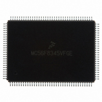
MC56F8345VFGE Freescale Semiconductor, MC56F8345VFGE Datasheet - Page 123

MC56F8345VFGE
Manufacturer Part Number
MC56F8345VFGE
Description
IC DSP 16BIT 60MHZ 128-LQFP
Manufacturer
Freescale Semiconductor
Series
56F8xxxr
Datasheet
1.MC56F8145VFGE.pdf
(172 pages)
Specifications of MC56F8345VFGE
Core Processor
56800
Core Size
16-Bit
Speed
60MHz
Connectivity
CAN, EBI/EMI, SCI, SPI
Peripherals
POR, PWM, Temp Sensor, WDT
Number Of I /o
49
Program Memory Size
136KB (68K x 16)
Program Memory Type
FLASH
Ram Size
6K x 16
Voltage - Supply (vcc/vdd)
2.25 V ~ 3.6 V
Data Converters
A/D 16x12b
Oscillator Type
External
Operating Temperature
-40°C ~ 105°C
Package / Case
128-LQFP
Data Bus Width
16 bit
Processor Series
MC56F83xx
Core
56800E
Numeric And Arithmetic Format
Fixed-Point
Device Million Instructions Per Second
60 MIPs
Maximum Clock Frequency
60 MHz
Number Of Programmable I/os
49
Data Ram Size
8 KB
Maximum Operating Temperature
+ 105 C
Mounting Style
SMD/SMT
Interface Type
SCI, SPI, CAN
Minimum Operating Temperature
- 40 C
For Use With
MC56F8367EVME - EVAL BOARD FOR MC56F83X
Lead Free Status / RoHS Status
Lead free / RoHS Compliant
Eeprom Size
-
Lead Free Status / Rohs Status
Lead free / RoHS Compliant
Available stocks
Company
Part Number
Manufacturer
Quantity
Price
Company:
Part Number:
MC56F8345VFGE
Manufacturer:
Freescale Semiconductor
Quantity:
1 985
Company:
Part Number:
MC56F8345VFGE
Manufacturer:
MOTOLOLA
Quantity:
245
Company:
Part Number:
MC56F8345VFGE
Manufacturer:
Freescale Semiconductor
Quantity:
10 000
Flash Access Blocking Mechanisms
The LOCKOUT_RECOVERY instruction has an associated 7-bit Data Register (DR) that is used to
control the clock divider circuit within the FM module. This divider, FM_CLKDIV[6:0], is used to control
the period of the clock used for timed events in the FM erase algorithm. This register must be set with
appropriate values before the lockout sequence can begin. Refer to the JTAG section of the 56F8300
Peripheral User Manual for more details on setting this register value.
The value of the JTAG FM_CLKDIV[6:0] will replace the value of the FM register FMCLKD that divides
down the system clock for timed events, as illustrated in
Figure
7-1. FM_CLKDIV[6] will map to the
PRDIV8 bit, and FM_CLKDIV[5:0] will map to the DIV[5:0] bits. The combination of PRDIV8 and DIV
must divide the FM input clock down to a frequency of 150kHz-200kHz. The “Writing the FMCLKD
Register” section in the Flash Memory chapter of the 56F8300 Peripheral User Manual gives specific
equations for calculating the correct values.
Flash Memory
SYS_CLK
input
DIVIDER
clock
2
7
FMCLKD
7
7
FM_CLKDIV
JTAG
FM_ERASE
Figure 7-1 JTAG to FM Connection for Lockout Recovery
Two examples of FM_CLKDIV calculations follow.
56F8345 Technical Data, Rev. 17
Freescale Semiconductor
123
Preliminary


