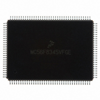
MC56F8345VFGE Freescale Semiconductor, MC56F8345VFGE Datasheet - Page 29

MC56F8345VFGE
Manufacturer Part Number
MC56F8345VFGE
Description
IC DSP 16BIT 60MHZ 128-LQFP
Manufacturer
Freescale Semiconductor
Series
56F8xxxr
Datasheet
1.MC56F8145VFGE.pdf
(172 pages)
Specifications of MC56F8345VFGE
Core Processor
56800
Core Size
16-Bit
Speed
60MHz
Connectivity
CAN, EBI/EMI, SCI, SPI
Peripherals
POR, PWM, Temp Sensor, WDT
Number Of I /o
49
Program Memory Size
136KB (68K x 16)
Program Memory Type
FLASH
Ram Size
6K x 16
Voltage - Supply (vcc/vdd)
2.25 V ~ 3.6 V
Data Converters
A/D 16x12b
Oscillator Type
External
Operating Temperature
-40°C ~ 105°C
Package / Case
128-LQFP
Data Bus Width
16 bit
Processor Series
MC56F83xx
Core
56800E
Numeric And Arithmetic Format
Fixed-Point
Device Million Instructions Per Second
60 MIPs
Maximum Clock Frequency
60 MHz
Number Of Programmable I/os
49
Data Ram Size
8 KB
Maximum Operating Temperature
+ 105 C
Mounting Style
SMD/SMT
Interface Type
SCI, SPI, CAN
Minimum Operating Temperature
- 40 C
For Use With
MC56F8367EVME - EVAL BOARD FOR MC56F83X
Lead Free Status / RoHS Status
Lead free / RoHS Compliant
Eeprom Size
-
Lead Free Status / Rohs Status
Lead free / RoHS Compliant
Available stocks
Company
Part Number
Manufacturer
Quantity
Price
Company:
Part Number:
MC56F8345VFGE
Manufacturer:
Freescale Semiconductor
Quantity:
1 985
Company:
Part Number:
MC56F8345VFGE
Manufacturer:
MOTOLOLA
Quantity:
245
Company:
Part Number:
MC56F8345VFGE
Manufacturer:
Freescale Semiconductor
Quantity:
10 000
Freescale Semiconductor
Preliminary
PHASEA1
PHASEB1
(GPIOC0)
(GPIOC1)
(SCLK1)
(MOSI1)
Signal
Name
(TB0)
(TB1)
Table 2-2 Signal and Package Information for the 128-Pin LQFP
Pin No.
10
9
Schmitt
Schmitt
Schmitt
Schmitt
Schmitt
Schmitt
Schmitt
Schmitt
Output
Output
Output
Output
Output
Output
Input/
Input/
Input/
Input/
Input/
Input/
Type
Input
Input
56F8345 Technical Data, Rev. 17
enabled
enabled
During
pull-up
pull-up
Reset
Input,
Input,
State
Phase A1 — Quadrature Decoder 1, PHASEA input for decoder
1.
TB0 — Timer B, Channel 0
SPI 1 Serial Clock — In the master mode, this pin serves as an
output, clocking slaved listeners. In slave mode, this pin serves
as the data clock input. To activate the SPI function, set the
PHSA_ALT bit in the SIM_GPS register. For details, see
6.5.8.
Port C GPIO — This GPIO pin can be individually programmed
as an input or output pin.
In the 56F8345, the default state after reset is PHASEA1.
In the 56F8145, the default state is not one of the functions
offered and must be reconfigured.
To deactivate the internal pull-up resistor, clear bit 0 in the
GPIOC_PUR register.
Phase B1 — Quadrature Decoder 1, PHASEB input for decoder
1.
TB1 — Timer B, Channel 1
SPI 1 Master Out/Slave In — This serial data pin is an output
from a master device and an input to a slave device. The master
device places data on the MOSI line a half-cycle before the clock
edge the slave device uses to latch the data. To activate the SPI
function, set the PHSB_ALT bit in the SIM_GPS register. For
details, see
Port C GPIO — This GPIO pin can be individually programmed
as an input or output pin.
In the 56F8345, the default state after reset is PHASEB1.
In the 56F8145, the default state is not one of the functions
offered and must be reconfigured.
To deactivate the internal pull-up resistor, clear bit 1 in the
GPIOC_PUR register.
Part
6.5.8.
Signal Description
Signal Pins
Part
29


