MC56F8345VFGE Freescale Semiconductor, MC56F8345VFGE Datasheet - Page 6
MC56F8345VFGE
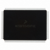
Manufacturer Part Number
MC56F8345VFGE
Description
IC DSP 16BIT 60MHZ 128-LQFP
Manufacturer
Freescale Semiconductor
Series
56F8xxxr
Datasheet
1.MC56F8145VFGE.pdf
(172 pages)
Specifications of MC56F8345VFGE
Core Processor
56800
Core Size
16-Bit
Speed
60MHz
Connectivity
CAN, EBI/EMI, SCI, SPI
Peripherals
POR, PWM, Temp Sensor, WDT
Number Of I /o
49
Program Memory Size
136KB (68K x 16)
Program Memory Type
FLASH
Ram Size
6K x 16
Voltage - Supply (vcc/vdd)
2.25 V ~ 3.6 V
Data Converters
A/D 16x12b
Oscillator Type
External
Operating Temperature
-40°C ~ 105°C
Package / Case
128-LQFP
Data Bus Width
16 bit
Processor Series
MC56F83xx
Core
56800E
Numeric And Arithmetic Format
Fixed-Point
Device Million Instructions Per Second
60 MIPs
Maximum Clock Frequency
60 MHz
Number Of Programmable I/os
49
Data Ram Size
8 KB
Maximum Operating Temperature
+ 105 C
Mounting Style
SMD/SMT
Interface Type
SCI, SPI, CAN
Minimum Operating Temperature
- 40 C
For Use With
MC56F8367EVME - EVAL BOARD FOR MC56F83X
Lead Free Status / RoHS Status
Lead free / RoHS Compliant
Eeprom Size
-
Lead Free Status / Rohs Status
Lead free / RoHS Compliant
Available stocks
Company
Part Number
Manufacturer
Quantity
Price
Company:

Part Number:
MC56F8345VFGE
Manufacturer:
Freescale Semiconductor
Quantity:
1 985
Company:
Part Number:
MC56F8345VFGE
Manufacturer:
MOTOLOLA
Quantity:
245
Company:
Part Number:
MC56F8345VFGE
Manufacturer:
Freescale Semiconductor
Quantity:
10 000


Part 1 Overview . . . . . . . . . . . . . . . . . . . . . . . . 7
Part 2 Signal/Connection Descriptions . . . . 17
Part 3 On-Chip Clock Synthesis (OCCS) . . . 36
Part 4 Memory Map . . . . . . . . . . . . . . . . . . . . 38
Part 5 Interrupt Controller (ITCN) . . . . . . . . . 74
Part 6 System Integration Module (SIM) . . 104
Part 7 Security Features . . . . . . . . . . . . . . . 121
6
1.1
1.2
1.3
1.4
1.5
1.6
2.1
2.2
3.1
3.2
3.3
4.1
4.2
4.3
4.4
4.5
4.6
4.7
4.8
5.1
5.2
5.3
5.4
5.5
5.6
5.7
6.1
6.2
6.3
6.4
6.5
6.6
6.7
6.8
6.9
7.1
7.2
56F8345/56F8145 Features . . . . . . . . . . . .7
Device Description. . . . . . . . . . . . . . . . . . . .9
Award-Winning Development Environment11
Architecture Block Diagram . . . . . . . . . . . .12
Product Documentation . . . . . . . . . . . . . . .16
Data Sheet Conventions . . . . . . . . . . . . . .16
Introduction . . . . . . . . . . . . . . . . . . . . . . . .17
Signal Pins. . . . . . . . . . . . . . . . . . . . . . . . .20
Introduction . . . . . . . . . . . . . . . . . . . . . . . .36
External Clock Operation. . . . . . . . . . . . . .36
Registers . . . . . . . . . . . . . . . . . . . . . . . . . .38
Introduction . . . . . . . . . . . . . . . . . . . . . . . .38
Program Map . . . . . . . . . . . . . . . . . . . . . . .39
Interrupt Vector Table . . . . . . . . . . . . . . . .41
Data Map . . . . . . . . . . . . . . . . . . . . . . . . . .45
Flash Memory Map . . . . . . . . . . . . . . . . . .45
EOnCE Memory Map. . . . . . . . . . . . . . . . .46
Peripheral Memory Mapped Registers . . .47
Factory Programmed Memory . . . . . . . . . .73
Introduction . . . . . . . . . . . . . . . . . . . . . . . .74
Features. . . . . . . . . . . . . . . . . . . . . . . . . . .74
Functional Description . . . . . . . . . . . . . . . .74
Block Diagram . . . . . . . . . . . . . . . . . . . . . .76
Operating Modes . . . . . . . . . . . . . . . . . . . .76
Register Descriptions. . . . . . . . . . . . . . . . .77
Resets . . . . . . . . . . . . . . . . . . . . . . . . . . .103
Introduction . . . . . . . . . . . . . . . . . . . . . . .104
Features. . . . . . . . . . . . . . . . . . . . . . . . . .104
Operating Modes . . . . . . . . . . . . . . . . . . .105
Operating Mode Register. . . . . . . . . . . . .105
Register Descriptions. . . . . . . . . . . . . . . .106
Clock Generation Overview . . . . . . . . . . .119
Power-Down Modes Overview . . . . . . . .119
Stop and Wait Mode Disable Function . .120
Resets . . . . . . . . . . . . . . . . . . . . . . . . . . .121
Operation with Security Enabled . . . . . . .121
Flash Access Blocking Mechanisms . . . .122
56F8345 Technical Data, Rev. 17
Table of Contents
Part 8 General Purpose Input/Output
(GPIO) . . . . . . . . . . . . . . . . . . . . . . . . . . . . . 125
Part 9 Joint Test Action Group (JTAG) . . 131
Part 10 Specifications . . . . . . . . . . . . . . . . 131
Part 11 Packaging . . . . . . . . . . . . . . . . . . . 158
Part 12 Design Considerations . . . . . . . . . 167
Part 13 Ordering Information . . . . . . . . . . 170
8.1
8.2
8.3
9.1
10.1
10.2
10.3
10.4
10.5
10.6
10.7
10.8
10.9
10.10
10.11
10.12
10.13
10.14
10.15
10.16
10.17
11.1
11.2
12.1
12.2
12.3
Introduction . . . . . . . . . . . . . . . . . . . . . . . 125
Memory Maps . . . . . . . . . . . . . . . . . . . . . 125
Configuration. . . . . . . . . . . . . . . . . . . . . . 125
JTAG Information . . . . . . . . . . . . . . . . . . 131
General Characteristics. . . . . . . . . . . . . . 131
DC Electrical Characteristics. . . . . . . . . . 136
AC Electrical Characteristics . . . . . . . . . . 140
Flash Memory Characteristics. . . . . . . . . 140
External Clock Operation Timing . . . . . . 141
Phase Locked Loop Timing. . . . . . . . . . . 141
Crystal Oscillator Timing . . . . . . . . . . . . . 142
Reset, Stop, Wait, Mode Select, and
Serial Peripheral Interface (SPI)
Quad Timer Timing . . . . . . . . . . . . . . . . . 148
Quadrature Decoder Timing . . . . . . . . . . 148
Serial Communication Interface (SCI)
Controller Area Network (CAN) Timing . . 150
JTAG Timing . . . . . . . . . . . . . . . . . . . . . . 150
Analog-to-Digital Converter (ADC)
Equivalent Circuit for ADC Inputs . . . . . . 155
Power Consumption . . . . . . . . . . . . . . . . 156
56F8345 Package and Pin-Out
56F8145 Package and Pin-Out
Thermal Design Considerations . . . . . . . 167
Electrical Design Considerations . . . . . . 168
Power Distribution and I/O Ring
Interrupt Timing . . . . . . . . . . . . . . . 142
Timing. . . . . . . . . . . . . . . . . . . . . . . 144
Timing. . . . . . . . . . . . . . . . . . . . . . . 149
Parameters . . . . . . . . . . . . . . . . . . . 152
Information . . . . . . . . . . . . . . . . . . . 158
Information . . . . . . . . . . . . . . . . . . . 161
Implementation . . . . . . . . . . . . . . . . 169
Freescale Semiconductor
Preliminary
Related parts for MC56F8345VFGE
Image
Part Number
Description
Manufacturer
Datasheet
Request
R

Part Number:
Description:
Manufacturer:
Freescale Semiconductor, Inc
Datasheet:
Part Number:
Description:
Manufacturer:
Freescale Semiconductor, Inc
Datasheet:
Part Number:
Description:
Manufacturer:
Freescale Semiconductor, Inc
Datasheet:
Part Number:
Description:
Manufacturer:
Freescale Semiconductor, Inc
Datasheet:
Part Number:
Description:
Manufacturer:
Freescale Semiconductor, Inc
Datasheet:
Part Number:
Description:
Manufacturer:
Freescale Semiconductor, Inc
Datasheet:
Part Number:
Description:
Manufacturer:
Freescale Semiconductor, Inc
Datasheet:
Part Number:
Description:
Manufacturer:
Freescale Semiconductor, Inc
Datasheet:
Part Number:
Description:
Manufacturer:
Freescale Semiconductor, Inc
Datasheet:
Part Number:
Description:
Manufacturer:
Freescale Semiconductor, Inc
Datasheet:
Part Number:
Description:
Manufacturer:
Freescale Semiconductor, Inc
Datasheet:
Part Number:
Description:
Manufacturer:
Freescale Semiconductor, Inc
Datasheet:
Part Number:
Description:
Manufacturer:
Freescale Semiconductor, Inc
Datasheet:
Part Number:
Description:
Manufacturer:
Freescale Semiconductor, Inc
Datasheet:
Part Number:
Description:
Manufacturer:
Freescale Semiconductor, Inc
Datasheet: