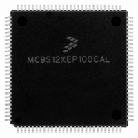
MC9S12XEP100CAL Freescale Semiconductor, MC9S12XEP100CAL Datasheet - Page 1077

MC9S12XEP100CAL
Manufacturer Part Number
MC9S12XEP100CAL
Description
IC MCU 16BIT 1M FLASH 112-LQFP
Manufacturer
Freescale Semiconductor
Series
HCS12r
Datasheet
1.MC9S12XEP768CAL.pdf
(1328 pages)
Specifications of MC9S12XEP100CAL
Core Processor
HCS12X
Core Size
16-Bit
Speed
50MHz
Connectivity
CAN, EBI/EMI, I²C, IrDA, SCI, SPI
Peripherals
LVD, POR, PWM, WDT
Number Of I /o
91
Program Memory Size
1MB (1M x 8)
Program Memory Type
FLASH
Eeprom Size
4K x 8
Ram Size
64K x 8
Voltage - Supply (vcc/vdd)
1.72 V ~ 5.5 V
Data Converters
A/D 16x12b
Oscillator Type
External
Operating Temperature
-40°C ~ 85°C
Package / Case
112-LQFP
Processor Series
S12XE
Core
HCS12
Data Bus Width
16 bit
Data Ram Size
64 KB
Interface Type
CAN/SCI/SPI
Maximum Clock Frequency
50 MHz
Number Of Programmable I/os
91
Number Of Timers
25
Maximum Operating Temperature
+ 85 C
Mounting Style
SMD/SMT
3rd Party Development Tools
EWHCS12
Development Tools By Supplier
KIT33812ECUEVME, EVB9S12XEP100, DEMO9S12XEP100
Minimum Operating Temperature
- 40 C
On-chip Adc
16-ch x 12-bit
Package
112LQFP
Family Name
HCS12X
Maximum Speed
50 MHz
Operating Supply Voltage
1.8|2.8|5 V
For Use With
EVB9S12XEP100 - BOARD EVAL FOR MC9S12XEP100DEMO9S12XEP100 - BOARD DEMO FOR MC9S12XEP100
Lead Free Status / RoHS Status
Lead free / RoHS Compliant
Available stocks
Company
Part Number
Manufacturer
Quantity
Price
Company:
Part Number:
MC9S12XEP100CAL
Manufacturer:
TOSHIBA
Quantity:
72
Company:
Part Number:
MC9S12XEP100CAL
Manufacturer:
Freescale Semiconductor
Quantity:
10 000
- Current page: 1077 of 1328
- Download datasheet (9Mb)
(0x7F_FF0F). The Verify Backdoor Access Key command sequence has no effect on the program and
erase protections defined in the Flash protection register, FPROT.
27.5.2
The MCU can be unsecured in special single chip mode by erasing the P-Flash and D-Flash memory by
one of the following methods:
After the CCIF flag sets to indicate that the Erase All Blocks operation has completed, reset the MCU into
special single chip mode. The BDM will execute the Erase Verify All Blocks command write sequence to
verify that the P-Flash and D-Flash memory is erased. If the P-Flash and D-Flash memory are verified as
erased the MCU will be unsecured. All BDM commands will be enabled and the Flash security byte may
be programmed to the unsecure state by the following method:
27.5.3
The availability of Flash module commands depends on the MCU operating mode and security state as
shown in
27.6
On each system reset the Flash module executes a reset sequence which establishes initial values for the
Flash Block Configuration Parameters, the FPROT and DFPROT protection registers, and the FOPT and
FSEC registers. The Flash module reverts to built-in default values that leave the module in a fully
protected and secured state if errors are encountered during execution of the reset sequence. If a double bit
fault is detected during the reset sequence, both MGSTAT bits in the FSTAT register will be set. The
ACCERR bit in the FSTAT register is set if errors are encountered while initializing the EEE buffer ram
during the reset sequence.
CCIF remains clear throughout the reset sequence. The Flash module holds off all CPU access for the
initial portion of the reset sequence. While Flash reads are possible when the hold is removed, writes to
the FCCOBIX, FCCOBHI, and FCCOBLO registers are ignored to prevent command activity while the
Memory Controller remains busy. Completion of the reset sequence is marked by setting CCIF high which
enables writes to the FCCOBIX, FCCOBHI, and FCCOBLO registers to launch any available Flash
command.
If a reset occurs while any Flash command is in progress, that command will be immediately aborted. The
state of the word being programmed or the sector/block being erased is not guaranteed.
Freescale Semiconductor
•
•
•
Reset the MCU into special single chip mode, delay while the erase test is performed by the BDM,
send BDM commands to disable protection in the P-Flash and D-Flash memory, and execute the
Erase All Blocks command write sequence to erase the P-Flash and D-Flash memory.
Reset the MCU into special expanded wide mode, disable protection in the P-Flash and D-Flash
memory and run code from external memory to execute the Erase All Blocks command write
sequence to erase the P-Flash and D-Flash memory.
Send BDM commands to execute a ‘Program P-Flash’ command sequence to program the Flash
security byte to the unsecured state and reset the MCU.
Table
Initialization
Unsecuring the MCU in Special Single Chip Mode using BDM
Mode and Security Effects on Flash Command Availability
27-30.
MC9S12XE-Family Reference Manual , Rev. 1.23
Chapter 27 512 KByte Flash Module (S12XFTM512K3V1)
1077
Related parts for MC9S12XEP100CAL
Image
Part Number
Description
Manufacturer
Datasheet
Request
R
Part Number:
Description:
Manufacturer:
Freescale Semiconductor, Inc
Datasheet:
Part Number:
Description:
Manufacturer:
Freescale Semiconductor, Inc
Datasheet:
Part Number:
Description:
Manufacturer:
Freescale Semiconductor, Inc
Datasheet:
Part Number:
Description:
Manufacturer:
Freescale Semiconductor, Inc
Datasheet:
Part Number:
Description:
Manufacturer:
Freescale Semiconductor, Inc
Datasheet:
Part Number:
Description:
Manufacturer:
Freescale Semiconductor, Inc
Datasheet:
Part Number:
Description:
Manufacturer:
Freescale Semiconductor, Inc
Datasheet:
Part Number:
Description:
Manufacturer:
Freescale Semiconductor, Inc
Datasheet:
Part Number:
Description:
Manufacturer:
Freescale Semiconductor, Inc
Datasheet:
Part Number:
Description:
Manufacturer:
Freescale Semiconductor, Inc
Datasheet:
Part Number:
Description:
Manufacturer:
Freescale Semiconductor, Inc
Datasheet:
Part Number:
Description:
Manufacturer:
Freescale Semiconductor, Inc
Datasheet:
Part Number:
Description:
Manufacturer:
Freescale Semiconductor, Inc
Datasheet:
Part Number:
Description:
Manufacturer:
Freescale Semiconductor, Inc
Datasheet:
Part Number:
Description:
Manufacturer:
Freescale Semiconductor, Inc
Datasheet:


