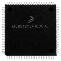
MC9S12XEP100CAL Freescale Semiconductor, MC9S12XEP100CAL Datasheet - Page 1206

MC9S12XEP100CAL
Manufacturer Part Number
MC9S12XEP100CAL
Description
IC MCU 16BIT 1M FLASH 112-LQFP
Manufacturer
Freescale Semiconductor
Series
HCS12r
Datasheet
1.MC9S12XEP768CAL.pdf
(1328 pages)
Specifications of MC9S12XEP100CAL
Core Processor
HCS12X
Core Size
16-Bit
Speed
50MHz
Connectivity
CAN, EBI/EMI, I²C, IrDA, SCI, SPI
Peripherals
LVD, POR, PWM, WDT
Number Of I /o
91
Program Memory Size
1MB (1M x 8)
Program Memory Type
FLASH
Eeprom Size
4K x 8
Ram Size
64K x 8
Voltage - Supply (vcc/vdd)
1.72 V ~ 5.5 V
Data Converters
A/D 16x12b
Oscillator Type
External
Operating Temperature
-40°C ~ 85°C
Package / Case
112-LQFP
Processor Series
S12XE
Core
HCS12
Data Bus Width
16 bit
Data Ram Size
64 KB
Interface Type
CAN/SCI/SPI
Maximum Clock Frequency
50 MHz
Number Of Programmable I/os
91
Number Of Timers
25
Maximum Operating Temperature
+ 85 C
Mounting Style
SMD/SMT
3rd Party Development Tools
EWHCS12
Development Tools By Supplier
KIT33812ECUEVME, EVB9S12XEP100, DEMO9S12XEP100
Minimum Operating Temperature
- 40 C
On-chip Adc
16-ch x 12-bit
Package
112LQFP
Family Name
HCS12X
Maximum Speed
50 MHz
Operating Supply Voltage
1.8|2.8|5 V
For Use With
EVB9S12XEP100 - BOARD EVAL FOR MC9S12XEP100DEMO9S12XEP100 - BOARD DEMO FOR MC9S12XEP100
Lead Free Status / RoHS Status
Lead free / RoHS Compliant
Available stocks
Company
Part Number
Manufacturer
Quantity
Price
Company:
Part Number:
MC9S12XEP100CAL
Manufacturer:
TOSHIBA
Quantity:
72
Company:
Part Number:
MC9S12XEP100CAL
Manufacturer:
Freescale Semiconductor
Quantity:
10 000
- Current page: 1206 of 1328
- Download datasheet (9Mb)
Appendix A Electrical Characteristics
maximum-rated voltages to this high-impedance circuit. Reliability of operation is enhanced if unused
inputs are tied to an appropriate logic voltage level (e.g., either V
1
2
3
4
5
A.1.6
All ESD testing is in conformity with CDF-AEC-Q100 stress test qualification for automotive grade
integrated circuits. During the device qualification ESD stresses were performed for the Human Body
Model (HBM) and the Charge Device Model.
A device will be defined as a failure if after exposure to ESD pulses the device no longer meets the device
specification. Complete DC parametric and functional testing is performed per the applicable device
1206
Num
Beyond absolute maximum ratings device might be damaged.
The device contains an internal voltage regulator to generate the logic and PLL supply out of the I/O supply. The absolute
maximum ratings apply when the device is powered from an external source.
All digital I/O pins are internally clamped to V
Those pins are internally clamped to V
This pin is clamped low to V
10
11
12
13
14
15
1
2
3
4
5
6
7
8
9
I/O, regulator and analog supply voltage
Digital logic supply voltage
PLL supply voltage
NVM supply voltage
Voltage difference V
Voltage difference V
Digital I/O input voltage
Analog reference
EXTAL, XTAL
TEST input
Instantaneous maximum current
Instantaneous maximum current
Instantaneous maximum current
Maximum current
Storage temperature range
Single pin limit for all digital I/O pins
Single pin limit for EXTAL, XTAL
Single pin limit for TEST
Single pin limit for power supply pins
ESD Protection and Latch-up Immunity
2
2
DDX
SSX
SSPLL
to V
to V
, but not clamped high. This pin must be tied low in applications.
2
5
MC9S12XE-Family Reference Manual , Rev. 1.23
SSA
DDA
Rating
Table A-1. Absolute Maximum Ratings
SSPLL
4
and V
SSX
3
and V
DDPLL
DDX
.
, or V
SSA
and V
DDA
SS35
V
Symbol
V
∆
V
∆
RH,
V
V
.
DDPLL
T stg
V
V
VDDX
VSSX
V
DD35
TEST
I
I
I
DDF
I
DT
DV
DL
DD
ILV
D
IN
V
or V
1
RL
DD35
–0.25
–100
–0.3
–0.3
–0.3
–0.3
–6.0
–0.3
–0.3
–0.3
–0.3
–0.3
Min
–25
–25
–65
).
Freescale Semiconductor
+100
Max
2.16
2.16
2.16
10.0
+25
+25
155
6.0
3.6
0.3
0.3
6.0
6.0
0
Unit
mA
mA
mA
mA
°C
V
V
V
V
V
V
V
V
V
V
Related parts for MC9S12XEP100CAL
Image
Part Number
Description
Manufacturer
Datasheet
Request
R
Part Number:
Description:
Manufacturer:
Freescale Semiconductor, Inc
Datasheet:
Part Number:
Description:
Manufacturer:
Freescale Semiconductor, Inc
Datasheet:
Part Number:
Description:
Manufacturer:
Freescale Semiconductor, Inc
Datasheet:
Part Number:
Description:
Manufacturer:
Freescale Semiconductor, Inc
Datasheet:
Part Number:
Description:
Manufacturer:
Freescale Semiconductor, Inc
Datasheet:
Part Number:
Description:
Manufacturer:
Freescale Semiconductor, Inc
Datasheet:
Part Number:
Description:
Manufacturer:
Freescale Semiconductor, Inc
Datasheet:
Part Number:
Description:
Manufacturer:
Freescale Semiconductor, Inc
Datasheet:
Part Number:
Description:
Manufacturer:
Freescale Semiconductor, Inc
Datasheet:
Part Number:
Description:
Manufacturer:
Freescale Semiconductor, Inc
Datasheet:
Part Number:
Description:
Manufacturer:
Freescale Semiconductor, Inc
Datasheet:
Part Number:
Description:
Manufacturer:
Freescale Semiconductor, Inc
Datasheet:
Part Number:
Description:
Manufacturer:
Freescale Semiconductor, Inc
Datasheet:
Part Number:
Description:
Manufacturer:
Freescale Semiconductor, Inc
Datasheet:
Part Number:
Description:
Manufacturer:
Freescale Semiconductor, Inc
Datasheet:


