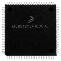
MC9S12XEP100CAL Freescale Semiconductor, MC9S12XEP100CAL Datasheet - Page 142

MC9S12XEP100CAL
Manufacturer Part Number
MC9S12XEP100CAL
Description
IC MCU 16BIT 1M FLASH 112-LQFP
Manufacturer
Freescale Semiconductor
Series
HCS12r
Datasheet
1.MC9S12XEP768CAL.pdf
(1328 pages)
Specifications of MC9S12XEP100CAL
Core Processor
HCS12X
Core Size
16-Bit
Speed
50MHz
Connectivity
CAN, EBI/EMI, I²C, IrDA, SCI, SPI
Peripherals
LVD, POR, PWM, WDT
Number Of I /o
91
Program Memory Size
1MB (1M x 8)
Program Memory Type
FLASH
Eeprom Size
4K x 8
Ram Size
64K x 8
Voltage - Supply (vcc/vdd)
1.72 V ~ 5.5 V
Data Converters
A/D 16x12b
Oscillator Type
External
Operating Temperature
-40°C ~ 85°C
Package / Case
112-LQFP
Processor Series
S12XE
Core
HCS12
Data Bus Width
16 bit
Data Ram Size
64 KB
Interface Type
CAN/SCI/SPI
Maximum Clock Frequency
50 MHz
Number Of Programmable I/os
91
Number Of Timers
25
Maximum Operating Temperature
+ 85 C
Mounting Style
SMD/SMT
3rd Party Development Tools
EWHCS12
Development Tools By Supplier
KIT33812ECUEVME, EVB9S12XEP100, DEMO9S12XEP100
Minimum Operating Temperature
- 40 C
On-chip Adc
16-ch x 12-bit
Package
112LQFP
Family Name
HCS12X
Maximum Speed
50 MHz
Operating Supply Voltage
1.8|2.8|5 V
For Use With
EVB9S12XEP100 - BOARD EVAL FOR MC9S12XEP100DEMO9S12XEP100 - BOARD DEMO FOR MC9S12XEP100
Lead Free Status / RoHS Status
Lead free / RoHS Compliant
Available stocks
Company
Part Number
Manufacturer
Quantity
Price
Company:
Part Number:
MC9S12XEP100CAL
Manufacturer:
TOSHIBA
Quantity:
72
Company:
Part Number:
MC9S12XEP100CAL
Manufacturer:
Freescale Semiconductor
Quantity:
10 000
- Current page: 142 of 1328
- Download datasheet (9Mb)
1. Read: Anytime.
Chapter 2 Port Integration Module (S12XEPIMV1)
2.3.46
142
Address 0x0259
Write:Never, writes to this register have no effect.
Field
PTP
PTP
PTP
PTP
Reset
3
2
1
0
W
R
Port P general purpose input/output data—Data Register
Port P pin 3 is associated with the PWM output channel 3 and the SS signal of SPI1.
The PWM function takes precedence over the SPI1 and the general purpose I/O function if the PWM channel 3 is
enabled. The SPI1 function takes precedence of the general purpose I/O function if the routed SPI1 is enabled.
When not used with the alternative functions, these pins can be used as general purpose I/O.
If the associated data direction bits of these pins are set to 1, a read returns the value of the port register, otherwise
the buffered pin input state is read.
Port P general purpose input/output data—Data Register
Port P pin 2 is associated with the PWM output channel 2 and the SCK signal of SPI1.
The PWM function takes precedence over the SPI1 and the general purpose I/O function if the PWM channel 2 is
enabled. The SPI1 function takes precedence of the general purpose I/O function if the routed SPI1 is enabled.
When not used with the alternative functions, these pins can be used as general purpose I/O.
If the associated data direction bits of these pins are set to 1, a read returns the value of the port register, otherwise
the buffered pin input state is read.
Port P general purpose input/output data—Data Register
Port P pin 1 is associated with the PWM output channel 1 and the MOSI signal of SPI1.
The PWM function takes precedence over the SPI1 and the general purpose I/O function if the PWM channel 1 is
enabled. The SPI1 function takes precedence of the general purpose I/O function if the routed SPI1 is enabled.
When not used with the alternative functions, these pins can be used as general purpose I/O.
If the associated data direction bits of these pins are set to 1, a read returns the value of the port register, otherwise
the buffered pin input state is read.
Port P general purpose input/output data—Data Register
Port P pin 0 is associated with the PWM output channel 0 and the MISO signal of SPI1.
The PWM function takes precedence over the SPI1 and the general purpose I/O function if the PWM channel 0 is
enabled. The SPI1 function takes precedence of the general purpose I/O function if the routed SPI1 is enabled.
When not used with the alternative functions, these pins can be used as general purpose I/O.
If the associated data direction bits of these pins are set to 1, a read returns the value of the port register, otherwise
the buffered pin input state is read.
PTIP7
Port P Input Register (PTIP)
u
7
= Unimplemented or Reserved
PTIP6
Table 2-41. PTP Register Field Descriptions (continued)
u
6
MC9S12XE-Family Reference Manual , Rev. 1.23
Figure 2-44. Port P Input Register (PTIP)
PTIP5
u
5
PTIP4
u
4
Description
u = Unaffected by reset
PTIP3
3
u
PTIP2
u
2
Freescale Semiconductor
PTIP1
u
1
Access: User read
PTIP0
u
0
(1)
Related parts for MC9S12XEP100CAL
Image
Part Number
Description
Manufacturer
Datasheet
Request
R
Part Number:
Description:
Manufacturer:
Freescale Semiconductor, Inc
Datasheet:
Part Number:
Description:
Manufacturer:
Freescale Semiconductor, Inc
Datasheet:
Part Number:
Description:
Manufacturer:
Freescale Semiconductor, Inc
Datasheet:
Part Number:
Description:
Manufacturer:
Freescale Semiconductor, Inc
Datasheet:
Part Number:
Description:
Manufacturer:
Freescale Semiconductor, Inc
Datasheet:
Part Number:
Description:
Manufacturer:
Freescale Semiconductor, Inc
Datasheet:
Part Number:
Description:
Manufacturer:
Freescale Semiconductor, Inc
Datasheet:
Part Number:
Description:
Manufacturer:
Freescale Semiconductor, Inc
Datasheet:
Part Number:
Description:
Manufacturer:
Freescale Semiconductor, Inc
Datasheet:
Part Number:
Description:
Manufacturer:
Freescale Semiconductor, Inc
Datasheet:
Part Number:
Description:
Manufacturer:
Freescale Semiconductor, Inc
Datasheet:
Part Number:
Description:
Manufacturer:
Freescale Semiconductor, Inc
Datasheet:
Part Number:
Description:
Manufacturer:
Freescale Semiconductor, Inc
Datasheet:
Part Number:
Description:
Manufacturer:
Freescale Semiconductor, Inc
Datasheet:
Part Number:
Description:
Manufacturer:
Freescale Semiconductor, Inc
Datasheet:


