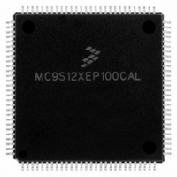
MC9S12XEP100CAL Freescale Semiconductor, MC9S12XEP100CAL Datasheet - Page 298

MC9S12XEP100CAL
Manufacturer Part Number
MC9S12XEP100CAL
Description
IC MCU 16BIT 1M FLASH 112-LQFP
Manufacturer
Freescale Semiconductor
Series
HCS12r
Datasheet
1.MC9S12XEP768CAL.pdf
(1328 pages)
Specifications of MC9S12XEP100CAL
Core Processor
HCS12X
Core Size
16-Bit
Speed
50MHz
Connectivity
CAN, EBI/EMI, I²C, IrDA, SCI, SPI
Peripherals
LVD, POR, PWM, WDT
Number Of I /o
91
Program Memory Size
1MB (1M x 8)
Program Memory Type
FLASH
Eeprom Size
4K x 8
Ram Size
64K x 8
Voltage - Supply (vcc/vdd)
1.72 V ~ 5.5 V
Data Converters
A/D 16x12b
Oscillator Type
External
Operating Temperature
-40°C ~ 85°C
Package / Case
112-LQFP
Processor Series
S12XE
Core
HCS12
Data Bus Width
16 bit
Data Ram Size
64 KB
Interface Type
CAN/SCI/SPI
Maximum Clock Frequency
50 MHz
Number Of Programmable I/os
91
Number Of Timers
25
Maximum Operating Temperature
+ 85 C
Mounting Style
SMD/SMT
3rd Party Development Tools
EWHCS12
Development Tools By Supplier
KIT33812ECUEVME, EVB9S12XEP100, DEMO9S12XEP100
Minimum Operating Temperature
- 40 C
On-chip Adc
16-ch x 12-bit
Package
112LQFP
Family Name
HCS12X
Maximum Speed
50 MHz
Operating Supply Voltage
1.8|2.8|5 V
For Use With
EVB9S12XEP100 - BOARD EVAL FOR MC9S12XEP100DEMO9S12XEP100 - BOARD DEMO FOR MC9S12XEP100
Lead Free Status / RoHS Status
Lead free / RoHS Compliant
Available stocks
Company
Part Number
Manufacturer
Quantity
Price
Company:
Part Number:
MC9S12XEP100CAL
Manufacturer:
TOSHIBA
Quantity:
72
Company:
Part Number:
MC9S12XEP100CAL
Manufacturer:
Freescale Semiconductor
Quantity:
10 000
- Current page: 298 of 1328
- Download datasheet (9Mb)
Chapter 7 Background Debug Module (S12XBDMV2)
Figure 7-10
there is up to a one clock-cycle delay from the host-generated falling edge on BKGD to the start of the bit
time as perceived by the target. The host initiates the bit time but the target finishes it. Since the target
wants the host to receive a logic 0, it drives the BKGD pin low for 13 target clock cycles then briefly drives
it high to speed up the rising edge. The host samples the bit level about 10 target clock cycles after starting
the bit time.
7.4.7
BDM commands that require CPU execution are ultimately treated at the MCU bus rate. Since the BDM
clock source can be asynchronously related to the bus frequency, when CLKSW = 0, it is very helpful to
provide a handshake protocol in which the host could determine when an issued command is executed by
the CPU. The alternative is to always wait the amount of time equal to the appropriate number of cycles at
the slowest possible rate the clock could be running. This sub-section will describe the hardware
handshake protocol.
The hardware handshake protocol signals to the host controller when an issued command was successfully
executed by the target. This protocol is implemented by a 16 serial clock cycle low pulse followed by a
brief speedup pulse in the BKGD pin. This pulse is generated by the target MCU when a command, issued
by the host, has been successfully executed (see
After the ACK pulse has finished: the host can start the bit retrieval if the last issued command was a read
command, or start a new command if the last command was a write command or a control command
(BACKGROUND, GO, GO_UNTIL or TRACE1). The ACK pulse is not issued earlier than 32 serial clock
cycles after the BDM command was issued. The end of the BDM command is assumed to be the 16th tick
of the last bit. This minimum delay assures enough time for the host to perceive the ACK pulse. Note also
that, there is no upper limit for the delay between the command and the related ACK pulse, since the
command execution depends upon the CPU bus frequency, which in some cases could be very slow
298
Start of Bit Time
Because of an order from the United States International Trade Commission, BGA-packaged product lines and partnumbers
Speedup Pulse
Target System
(Target MCU)
indicated here currently are not available from Freescale for import or sale in the United States prior to September 2010
BDM Clock
BKGD Pin
BKGD Pin
Perceived
Drive and
Drive to
Host
Serial Interface Hardware Handshake Protocol
shows the host receiving a logic 0 from the target. Since the host is asynchronous to the target,
Figure 7-10. BDM Target-to-Host Serial Bit Timing (Logic 0)
MC9S12XE-Family Reference Manual , Rev. 1.23
10 Cycles
10 Cycles
Figure
7-11). This pulse is referred to as the ACK pulse.
High-Impedance
Host Samples
BKGD Pin
Speedup Pulse
Freescale Semiconductor
Next Bit
Earliest
Start of
Related parts for MC9S12XEP100CAL
Image
Part Number
Description
Manufacturer
Datasheet
Request
R
Part Number:
Description:
Manufacturer:
Freescale Semiconductor, Inc
Datasheet:
Part Number:
Description:
Manufacturer:
Freescale Semiconductor, Inc
Datasheet:
Part Number:
Description:
Manufacturer:
Freescale Semiconductor, Inc
Datasheet:
Part Number:
Description:
Manufacturer:
Freescale Semiconductor, Inc
Datasheet:
Part Number:
Description:
Manufacturer:
Freescale Semiconductor, Inc
Datasheet:
Part Number:
Description:
Manufacturer:
Freescale Semiconductor, Inc
Datasheet:
Part Number:
Description:
Manufacturer:
Freescale Semiconductor, Inc
Datasheet:
Part Number:
Description:
Manufacturer:
Freescale Semiconductor, Inc
Datasheet:
Part Number:
Description:
Manufacturer:
Freescale Semiconductor, Inc
Datasheet:
Part Number:
Description:
Manufacturer:
Freescale Semiconductor, Inc
Datasheet:
Part Number:
Description:
Manufacturer:
Freescale Semiconductor, Inc
Datasheet:
Part Number:
Description:
Manufacturer:
Freescale Semiconductor, Inc
Datasheet:
Part Number:
Description:
Manufacturer:
Freescale Semiconductor, Inc
Datasheet:
Part Number:
Description:
Manufacturer:
Freescale Semiconductor, Inc
Datasheet:
Part Number:
Description:
Manufacturer:
Freescale Semiconductor, Inc
Datasheet:


