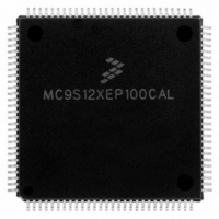
MC9S12XEP100CAL Freescale Semiconductor, MC9S12XEP100CAL Datasheet - Page 307

MC9S12XEP100CAL
Manufacturer Part Number
MC9S12XEP100CAL
Description
IC MCU 16BIT 1M FLASH 112-LQFP
Manufacturer
Freescale Semiconductor
Series
HCS12r
Datasheet
1.MC9S12XEP768CAL.pdf
(1328 pages)
Specifications of MC9S12XEP100CAL
Core Processor
HCS12X
Core Size
16-Bit
Speed
50MHz
Connectivity
CAN, EBI/EMI, I²C, IrDA, SCI, SPI
Peripherals
LVD, POR, PWM, WDT
Number Of I /o
91
Program Memory Size
1MB (1M x 8)
Program Memory Type
FLASH
Eeprom Size
4K x 8
Ram Size
64K x 8
Voltage - Supply (vcc/vdd)
1.72 V ~ 5.5 V
Data Converters
A/D 16x12b
Oscillator Type
External
Operating Temperature
-40°C ~ 85°C
Package / Case
112-LQFP
Processor Series
S12XE
Core
HCS12
Data Bus Width
16 bit
Data Ram Size
64 KB
Interface Type
CAN/SCI/SPI
Maximum Clock Frequency
50 MHz
Number Of Programmable I/os
91
Number Of Timers
25
Maximum Operating Temperature
+ 85 C
Mounting Style
SMD/SMT
3rd Party Development Tools
EWHCS12
Development Tools By Supplier
KIT33812ECUEVME, EVB9S12XEP100, DEMO9S12XEP100
Minimum Operating Temperature
- 40 C
On-chip Adc
16-ch x 12-bit
Package
112LQFP
Family Name
HCS12X
Maximum Speed
50 MHz
Operating Supply Voltage
1.8|2.8|5 V
For Use With
EVB9S12XEP100 - BOARD EVAL FOR MC9S12XEP100DEMO9S12XEP100 - BOARD DEMO FOR MC9S12XEP100
Lead Free Status / RoHS Status
Lead free / RoHS Compliant
Available stocks
Company
Part Number
Manufacturer
Quantity
Price
Company:
Part Number:
MC9S12XEP100CAL
Manufacturer:
TOSHIBA
Quantity:
72
Company:
Part Number:
MC9S12XEP100CAL
Manufacturer:
Freescale Semiconductor
Quantity:
10 000
- Current page: 307 of 1328
- Download datasheet (9Mb)
Chapter 8
S12X Debug (S12XDBGV3) Module
8.1
The S12XDBG module provides an on-chip trace buffer with flexible triggering capability to allow non-
intrusive debug of application software. The S12XDBG module is optimized for the S12X 16-bit
architecture and allows debugging of CPU12Xand XGATE module operations.
Typically the S12XDBG module is used in conjunction with the S12XBDM module, whereby the user
configures the S12XDBG module for a debugging session over the BDM interface. Once configured the
S12XDBG module is armed and the device leaves BDM Mode returning control to the user program,
which is then monitored by the S12XDBG module. Alternatively the S12XDBG module can be configured
over a serial interface using SWI routines.
8.1.1
Freescale Semiconductor
Revision
Because of an order from the United States International Trade Commission, BGA-packaged product lines and partnumbers
Number
V03.18
V03.19
V03.20
V03.21
V03.22
V03.23
V03.24
indicated here currently are not available from Freescale for import or sale in the United States prior to September 2010
Term
COF
BDM
DUG
Introduction
Revision Date
Glossary
12 Nov 2007
13 Nov 2007
20 Apr 2007
24 Apr 2007
14 Apr 2007
23 Oct 2007
04 Jan 2008
Change Of Flow.
Change in the program flow due to a conditional branch, indexed jump or interrupt
Background Debug Mode
Device User Guide, describing the features of the device into which the DBG is integrated
8.4.2.3/8-331
8.4.3.5/8-333
8.3.2.7/8-319
8.4.2.2/8-331
8.4.2.4/8-332
8.4.5.2/8-336
8.4.5.5/8-343
8.4.5.3/8-338
Sections
Affected
General
MC9S12XE-Family Reference Manual , Rev. 1.23
Table 8-2. Glossary Of Terms
Table 8-1. Revision History
- Added “Data Bus Comparison NDB Dependency” section
- Clarified effect TRIG has on state sequencer.
- Clarified simultaneous arm and disarm effect.
- Clarified reserved State Sequencer encodings.
- Added single databyte comparison limitation information
- Added statement about interrupt vector fetches whilst tagging.
- Removed LOOP1 tracing restriction NOTE.
- Added pin reset effect NOTE.
- Text readability improved, typo removed.
- Corrected bit name.
Definition
Description of Changes
307
Related parts for MC9S12XEP100CAL
Image
Part Number
Description
Manufacturer
Datasheet
Request
R
Part Number:
Description:
Manufacturer:
Freescale Semiconductor, Inc
Datasheet:
Part Number:
Description:
Manufacturer:
Freescale Semiconductor, Inc
Datasheet:
Part Number:
Description:
Manufacturer:
Freescale Semiconductor, Inc
Datasheet:
Part Number:
Description:
Manufacturer:
Freescale Semiconductor, Inc
Datasheet:
Part Number:
Description:
Manufacturer:
Freescale Semiconductor, Inc
Datasheet:
Part Number:
Description:
Manufacturer:
Freescale Semiconductor, Inc
Datasheet:
Part Number:
Description:
Manufacturer:
Freescale Semiconductor, Inc
Datasheet:
Part Number:
Description:
Manufacturer:
Freescale Semiconductor, Inc
Datasheet:
Part Number:
Description:
Manufacturer:
Freescale Semiconductor, Inc
Datasheet:
Part Number:
Description:
Manufacturer:
Freescale Semiconductor, Inc
Datasheet:
Part Number:
Description:
Manufacturer:
Freescale Semiconductor, Inc
Datasheet:
Part Number:
Description:
Manufacturer:
Freescale Semiconductor, Inc
Datasheet:
Part Number:
Description:
Manufacturer:
Freescale Semiconductor, Inc
Datasheet:
Part Number:
Description:
Manufacturer:
Freescale Semiconductor, Inc
Datasheet:
Part Number:
Description:
Manufacturer:
Freescale Semiconductor, Inc
Datasheet:


