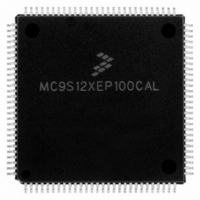
MC9S12XEP100CAL Freescale Semiconductor, MC9S12XEP100CAL Datasheet - Page 332

MC9S12XEP100CAL
Manufacturer Part Number
MC9S12XEP100CAL
Description
IC MCU 16BIT 1M FLASH 112-LQFP
Manufacturer
Freescale Semiconductor
Series
HCS12r
Datasheet
1.MC9S12XEP768CAL.pdf
(1328 pages)
Specifications of MC9S12XEP100CAL
Core Processor
HCS12X
Core Size
16-Bit
Speed
50MHz
Connectivity
CAN, EBI/EMI, I²C, IrDA, SCI, SPI
Peripherals
LVD, POR, PWM, WDT
Number Of I /o
91
Program Memory Size
1MB (1M x 8)
Program Memory Type
FLASH
Eeprom Size
4K x 8
Ram Size
64K x 8
Voltage - Supply (vcc/vdd)
1.72 V ~ 5.5 V
Data Converters
A/D 16x12b
Oscillator Type
External
Operating Temperature
-40°C ~ 85°C
Package / Case
112-LQFP
Processor Series
S12XE
Core
HCS12
Data Bus Width
16 bit
Data Ram Size
64 KB
Interface Type
CAN/SCI/SPI
Maximum Clock Frequency
50 MHz
Number Of Programmable I/os
91
Number Of Timers
25
Maximum Operating Temperature
+ 85 C
Mounting Style
SMD/SMT
3rd Party Development Tools
EWHCS12
Development Tools By Supplier
KIT33812ECUEVME, EVB9S12XEP100, DEMO9S12XEP100
Minimum Operating Temperature
- 40 C
On-chip Adc
16-ch x 12-bit
Package
112LQFP
Family Name
HCS12X
Maximum Speed
50 MHz
Operating Supply Voltage
1.8|2.8|5 V
For Use With
EVB9S12XEP100 - BOARD EVAL FOR MC9S12XEP100DEMO9S12XEP100 - BOARD DEMO FOR MC9S12XEP100
Lead Free Status / RoHS Status
Lead free / RoHS Compliant
Available stocks
Company
Part Number
Manufacturer
Quantity
Price
Company:
Part Number:
MC9S12XEP100CAL
Manufacturer:
TOSHIBA
Quantity:
72
Company:
Part Number:
MC9S12XEP100CAL
Manufacturer:
Freescale Semiconductor
Quantity:
10 000
- Current page: 332 of 1328
- Download datasheet (9Mb)
Chapter 8 S12X Debug (S12XDBGV3) Module
8.4.2.4
When using the AB comparator pair for a range comparison, the data bus can also be used for qualification
by using the comparator A data and data mask registers. Furthermore the DBGACTL RW and RWE bits
can be used to qualify the range comparison on either a read or a write access. The corresponding
DBGBCTL bits are ignored. Similarly when using the CD comparator pair for a range comparison, the
data bus can also be used for qualification by using the comparator C data and data mask registers.
Furthermore the DBGCCTL RW and RWE bits can be used to qualify the range comparison on either a
read or a write access if tagging is not selected. The corresponding DBGDCTL bits are ignored. The SZE
and SZ control bits are ignored in range mode. The comparator A and C TAG bits are used to tag range
comparisons for the AB and CD ranges respectively. The comparator B and D TAG bits are ignored in
range modes. In order for a range comparison using comparators A and B, both COMPEA and COMPEB
must be set; to disable range comparisons both must be cleared. Similarly for a range CD comparison, both
COMPEC and COMPED must be set. If a range mode is selected SRCA and SRCC select the source
(S12X or XGATE), SRCB and SRCD are ignored. The comparator A and C BRK bits are used for the AB
and CD ranges respectively, the comparator B and D BRK bits are ignored in range mode. When
configured for range comparisons and tagging, the ranges are accurate only to word boundaries.
8.4.2.4.1
In the Inside Range comparator mode, either comparator pair A and B or comparator pair C and D can be
configured for range comparisons by the control register (DBGC2). The match condition requires that a
valid match for both comparators happens on the same bus cycle. A match condition on only one
comparator is not valid. An aligned word access which straddles the range boundary will cause a trigger
only if the aligned address is inside the range.
8.4.2.4.2
In the Outside Range comparator mode, either comparator pair A and B or comparator pair C and D can
be configured for range comparisons. A single match condition on either of the comparators is recognized
as valid. An aligned word access which straddles the range boundary will cause a trigger only if the aligned
address is outside the range.
Outside range mode in combination with tagged triggers can be used to detect if the opcode fetches are
from an unexpected range. In forced trigger modes the outside range trigger would typically be activated
at any interrupt vector fetch or register access. This can be avoided by setting the upper or lower range limit
to $7FFFFF or $000000 respectively. Interrupt vector fetches do not cause taghits
332
Because of an order from the United States International Trade Commission, BGA-packaged product lines and partnumbers
indicated here currently are not available from Freescale for import or sale in the United States prior to September 2010
NDB
Range Comparisons
0
0
1
1
Inside Range (CompAC_Addr ≤ address ≤ CompBD_Addr)
Outside Range (address < CompAC_Addr or address > CompBD_Addr)
DBGxDHM[n] /
DBGxDLM[n]
0
1
0
1
Table 8-41. NDB and MASK bit dependency
MC9S12XE-Family Reference Manual , Rev. 1.23
Compare data bus bit. Match on equivalence.
Compare data bus bit. Match on difference.
Do not compare data bus bit.
Do not compare data bus bit.
Comment
Freescale Semiconductor
Related parts for MC9S12XEP100CAL
Image
Part Number
Description
Manufacturer
Datasheet
Request
R
Part Number:
Description:
Manufacturer:
Freescale Semiconductor, Inc
Datasheet:
Part Number:
Description:
Manufacturer:
Freescale Semiconductor, Inc
Datasheet:
Part Number:
Description:
Manufacturer:
Freescale Semiconductor, Inc
Datasheet:
Part Number:
Description:
Manufacturer:
Freescale Semiconductor, Inc
Datasheet:
Part Number:
Description:
Manufacturer:
Freescale Semiconductor, Inc
Datasheet:
Part Number:
Description:
Manufacturer:
Freescale Semiconductor, Inc
Datasheet:
Part Number:
Description:
Manufacturer:
Freescale Semiconductor, Inc
Datasheet:
Part Number:
Description:
Manufacturer:
Freescale Semiconductor, Inc
Datasheet:
Part Number:
Description:
Manufacturer:
Freescale Semiconductor, Inc
Datasheet:
Part Number:
Description:
Manufacturer:
Freescale Semiconductor, Inc
Datasheet:
Part Number:
Description:
Manufacturer:
Freescale Semiconductor, Inc
Datasheet:
Part Number:
Description:
Manufacturer:
Freescale Semiconductor, Inc
Datasheet:
Part Number:
Description:
Manufacturer:
Freescale Semiconductor, Inc
Datasheet:
Part Number:
Description:
Manufacturer:
Freescale Semiconductor, Inc
Datasheet:
Part Number:
Description:
Manufacturer:
Freescale Semiconductor, Inc
Datasheet:


