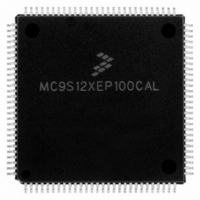
MC9S12XEP100CAL Freescale Semiconductor, MC9S12XEP100CAL Datasheet - Page 335

MC9S12XEP100CAL
Manufacturer Part Number
MC9S12XEP100CAL
Description
IC MCU 16BIT 1M FLASH 112-LQFP
Manufacturer
Freescale Semiconductor
Series
HCS12r
Datasheet
1.MC9S12XEP768CAL.pdf
(1328 pages)
Specifications of MC9S12XEP100CAL
Core Processor
HCS12X
Core Size
16-Bit
Speed
50MHz
Connectivity
CAN, EBI/EMI, I²C, IrDA, SCI, SPI
Peripherals
LVD, POR, PWM, WDT
Number Of I /o
91
Program Memory Size
1MB (1M x 8)
Program Memory Type
FLASH
Eeprom Size
4K x 8
Ram Size
64K x 8
Voltage - Supply (vcc/vdd)
1.72 V ~ 5.5 V
Data Converters
A/D 16x12b
Oscillator Type
External
Operating Temperature
-40°C ~ 85°C
Package / Case
112-LQFP
Processor Series
S12XE
Core
HCS12
Data Bus Width
16 bit
Data Ram Size
64 KB
Interface Type
CAN/SCI/SPI
Maximum Clock Frequency
50 MHz
Number Of Programmable I/os
91
Number Of Timers
25
Maximum Operating Temperature
+ 85 C
Mounting Style
SMD/SMT
3rd Party Development Tools
EWHCS12
Development Tools By Supplier
KIT33812ECUEVME, EVB9S12XEP100, DEMO9S12XEP100
Minimum Operating Temperature
- 40 C
On-chip Adc
16-ch x 12-bit
Package
112LQFP
Family Name
HCS12X
Maximum Speed
50 MHz
Operating Supply Voltage
1.8|2.8|5 V
For Use With
EVB9S12XEP100 - BOARD EVAL FOR MC9S12XEP100DEMO9S12XEP100 - BOARD DEMO FOR MC9S12XEP100
Lead Free Status / RoHS Status
Lead free / RoHS Compliant
Available stocks
Company
Part Number
Manufacturer
Quantity
Price
Company:
Part Number:
MC9S12XEP100CAL
Manufacturer:
TOSHIBA
Quantity:
72
Company:
Part Number:
MC9S12XEP100CAL
Manufacturer:
Freescale Semiconductor
Quantity:
10 000
- Current page: 335 of 1328
- Download datasheet (9Mb)
Chapter 8 S12X Debug (S12XDBGV3) Module
then state1 of the state sequencer is entered. Further transitions between the states are then controlled by
the state control registers and depend upon a selected trigger mode condition being met. From Final State
the only permitted transition is back to the disarmed state0. Transition between any of the states 1 to 3 is
not restricted. Each transition updates the SSF[2:0] flags in DBGSR accordingly to indicate the current
state.
Alternatively by setting the TRIG bit in DBGSC1, the state machine can be triggered to state0 or Final
State depending on tracing alignment.
A tag hit through TAGHI/TAGLO brings the state sequencer immediately into state0, causes a breakpoint,
if breakpoints are enabled, and ends tracing immediately independent of the trigger alignment bits
TALIGN[1:0].
Independent of the state sequencer, each comparator channel can be individually configured to generate an
immediate breakpoint when a match occurs through the use of the BRK bits in the DBGxCTL registers.
Thus it is possible to generate an immediate breakpoint on selected channels, whilst a state sequencer
transition can be initiated by a match on other channels. If a debug session is ended by a trigger on a
channel with BRK = 1, the state sequencer transitions through Final State for a clock cycle to state0. This
is independent of tracing and breakpoint activity, thus with tracing and breakpoints disabled, the state
sequencer enters state0 and the debug module is disarmed.
An XGATE S/W breakpoint request, if enabled causes a transition to the State0 and generates a breakpoint
request to the CPU12X immediately
8.4.4.1
Final State
On entering Final State a trigger may be issued to the trace buffer according to the trace position control
as defined by the TALIGN field (see
Section
8.3.2.3”). If TSOURCE in the trace control register DBGTCR
are cleared then the trace buffer is disabled and the transition to Final State can only generate a breakpoint
request. In this case or upon completion of a tracing session when tracing is enabled, the ARM bit in the
DBGC1 register is cleared, returning the module to the disarmed state0. If tracing is enabled, a breakpoint
request can occur at the end of the tracing session. If neither tracing nor breakpoints are enabled then when
the final state is reached it returns automatically to state0 and the debug module is disarmed.
8.4.5
Trace Buffer Operation
The trace buffer is a 64 lines deep by 64-bits wide RAM array. The S12XDBG module stores trace
information in the RAM array in a circular buffer format. The RAM array can be accessed through a
register window (DBGTBH:DBGTBL) using 16-bit wide word accesses. After each complete 64-bit trace
buffer line is read, an internal pointer into the RAM is incremented so that the next read will receive fresh
information. Data is stored in the format shown in
Table
8-43. After each store the counter register bits
DBGCNT[6:0] are incremented. Tracing of CPU12X activity is disabled when the BDM is active but
tracing of XGATE activity is still possible. Reading the trace buffer whilst the DBG is armed returns
invalid data and the trace buffer pointer is not incremented.
MC9S12XE-Family Reference Manual Rev. 1.23
Freescale Semiconductor
335
Because of an order from the United States International Trade Commission, BGA-packaged product lines and partnumbers
indicated here currently are not available from Freescale for import or sale in the United States prior to September 2010
Related parts for MC9S12XEP100CAL
Image
Part Number
Description
Manufacturer
Datasheet
Request
R
Part Number:
Description:
Manufacturer:
Freescale Semiconductor, Inc
Datasheet:
Part Number:
Description:
Manufacturer:
Freescale Semiconductor, Inc
Datasheet:
Part Number:
Description:
Manufacturer:
Freescale Semiconductor, Inc
Datasheet:
Part Number:
Description:
Manufacturer:
Freescale Semiconductor, Inc
Datasheet:
Part Number:
Description:
Manufacturer:
Freescale Semiconductor, Inc
Datasheet:
Part Number:
Description:
Manufacturer:
Freescale Semiconductor, Inc
Datasheet:
Part Number:
Description:
Manufacturer:
Freescale Semiconductor, Inc
Datasheet:
Part Number:
Description:
Manufacturer:
Freescale Semiconductor, Inc
Datasheet:
Part Number:
Description:
Manufacturer:
Freescale Semiconductor, Inc
Datasheet:
Part Number:
Description:
Manufacturer:
Freescale Semiconductor, Inc
Datasheet:
Part Number:
Description:
Manufacturer:
Freescale Semiconductor, Inc
Datasheet:
Part Number:
Description:
Manufacturer:
Freescale Semiconductor, Inc
Datasheet:
Part Number:
Description:
Manufacturer:
Freescale Semiconductor, Inc
Datasheet:
Part Number:
Description:
Manufacturer:
Freescale Semiconductor, Inc
Datasheet:
Part Number:
Description:
Manufacturer:
Freescale Semiconductor, Inc
Datasheet:


