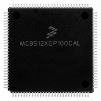
MC9S12XEP100CAL Freescale Semiconductor, MC9S12XEP100CAL Datasheet - Page 515

MC9S12XEP100CAL
Manufacturer Part Number
MC9S12XEP100CAL
Description
IC MCU 16BIT 1M FLASH 112-LQFP
Manufacturer
Freescale Semiconductor
Series
HCS12r
Datasheet
1.MC9S12XEP768CAL.pdf
(1328 pages)
Specifications of MC9S12XEP100CAL
Core Processor
HCS12X
Core Size
16-Bit
Speed
50MHz
Connectivity
CAN, EBI/EMI, I²C, IrDA, SCI, SPI
Peripherals
LVD, POR, PWM, WDT
Number Of I /o
91
Program Memory Size
1MB (1M x 8)
Program Memory Type
FLASH
Eeprom Size
4K x 8
Ram Size
64K x 8
Voltage - Supply (vcc/vdd)
1.72 V ~ 5.5 V
Data Converters
A/D 16x12b
Oscillator Type
External
Operating Temperature
-40°C ~ 85°C
Package / Case
112-LQFP
Processor Series
S12XE
Core
HCS12
Data Bus Width
16 bit
Data Ram Size
64 KB
Interface Type
CAN/SCI/SPI
Maximum Clock Frequency
50 MHz
Number Of Programmable I/os
91
Number Of Timers
25
Maximum Operating Temperature
+ 85 C
Mounting Style
SMD/SMT
3rd Party Development Tools
EWHCS12
Development Tools By Supplier
KIT33812ECUEVME, EVB9S12XEP100, DEMO9S12XEP100
Minimum Operating Temperature
- 40 C
On-chip Adc
16-ch x 12-bit
Package
112LQFP
Family Name
HCS12X
Maximum Speed
50 MHz
Operating Supply Voltage
1.8|2.8|5 V
For Use With
EVB9S12XEP100 - BOARD EVAL FOR MC9S12XEP100DEMO9S12XEP100 - BOARD DEMO FOR MC9S12XEP100
Lead Free Status / RoHS Status
Lead free / RoHS Compliant
Available stocks
Company
Part Number
Manufacturer
Quantity
Price
Company:
Part Number:
MC9S12XEP100CAL
Manufacturer:
TOSHIBA
Quantity:
72
Company:
Part Number:
MC9S12XEP100CAL
Manufacturer:
Freescale Semiconductor
Quantity:
10 000
- Current page: 515 of 1328
- Download datasheet (9Mb)
Freescale Semiconductor
Because of an order from the United States International Trade Commission, BGA-packaged product lines and partnumbers
S8C, S4C,
S2C, S1C
FRZ[1:0]
indicated here currently are not available from Freescale for import or sale in the United States prior to September 2010
Field
FIFO
6–3
1–0
2
Conversion Sequence Length — These bits control the number of conversions per sequence.
shows all combinations. At reset, S4C is set to 1 (sequence length is 4). This is to maintain software continuity
to HC12 family.
Result Register FIFO Mode — If this bit is zero (non-FIFO mode), the A/D conversion results map into the result
registers based on the conversion sequence; the result of the first conversion appears in the first result register
(ATDDR0), the second result in the second result register (ATDDR1), and so on.
If this bit is one (FIFO mode) the conversion counter is not reset at the beginning or ending of a conversion
sequence; sequential conversion results are placed in consecutive result registers. In a continuously scanning
conversion sequence, the result register counter will wrap around when it reaches the end of the result register
file. The conversion counter value (CC3-0 in ATDSTAT0) can be used to determine where in the result register
file, the current conversion result will be placed.
Aborting a conversion or starting a new conversion clears the conversion counter even if FIFO=1. So the first
result of a new conversion sequence, started by writing to ATDCTL5, will always be place in the first result register
(ATDDDR0). Intended usage of FIFO mode is continuos conversion (SCAN=1) or triggered conversion
(ETRIG=1).
Which result registers hold valid data can be tracked using the conversion complete flags. Fast flag clear mode
may or may not be useful in a particular application to track valid data.
If this bit is one, automatic compare of result registers is always disabled, that is ADC12B16C will behave as if
ACMPIE and all CPME[n] were zero.
0 Conversion results are placed in the corresponding result register up to the selected sequence length.
1 Conversion results are placed in consecutive result registers (wrap around at end).
Background Debug Freeze Enable — When debugging an application, it is useful in many cases to have the
ATD pause when a breakpoint (Freeze Mode) is encountered. These 2 bits determine how the ATD will respond
to a breakpoint as shown in
may compromise the accuracy of an immediately frozen conversion depending on the length of the freeze period.
V
RH
V
Input Signal
5.120 Volts
RL
= 5.12 Volts
0.022
0.020
0.018
0.016
0.014
0.012
0.010
0.008
0.006
0.004
0.003
0.002
0.000
= 0 Volts
...
Table 13-9. ATDCTL3 Field Descriptions (continued)
Table 13-10. Examples of ideal decimal ATD Results
MC9S12XE-Family Reference Manual Rev. 1.23
Table
(resolution=20mV)
13-12. Leakage onto the storage node and comparator reference capacitors
Codes
8-Bit
255
...
1
1
1
1
1
1
1
0
0
0
0
0
0
Description
(resolution=5mV)
Codes
10-Bit
1023
Chapter 13 Analog-to-Digital Converter (ADC12B16CV1)
...
4
4
4
3
3
2
2
2
1
1
0
0
0
(resolution=1.25mV)
(transfer curve has
1.25mV offset)
Codes
12-Bit
4095
17
16
14
12
11
...
9
8
6
4
3
2
1
0
Table 13-11
515
Related parts for MC9S12XEP100CAL
Image
Part Number
Description
Manufacturer
Datasheet
Request
R
Part Number:
Description:
Manufacturer:
Freescale Semiconductor, Inc
Datasheet:
Part Number:
Description:
Manufacturer:
Freescale Semiconductor, Inc
Datasheet:
Part Number:
Description:
Manufacturer:
Freescale Semiconductor, Inc
Datasheet:
Part Number:
Description:
Manufacturer:
Freescale Semiconductor, Inc
Datasheet:
Part Number:
Description:
Manufacturer:
Freescale Semiconductor, Inc
Datasheet:
Part Number:
Description:
Manufacturer:
Freescale Semiconductor, Inc
Datasheet:
Part Number:
Description:
Manufacturer:
Freescale Semiconductor, Inc
Datasheet:
Part Number:
Description:
Manufacturer:
Freescale Semiconductor, Inc
Datasheet:
Part Number:
Description:
Manufacturer:
Freescale Semiconductor, Inc
Datasheet:
Part Number:
Description:
Manufacturer:
Freescale Semiconductor, Inc
Datasheet:
Part Number:
Description:
Manufacturer:
Freescale Semiconductor, Inc
Datasheet:
Part Number:
Description:
Manufacturer:
Freescale Semiconductor, Inc
Datasheet:
Part Number:
Description:
Manufacturer:
Freescale Semiconductor, Inc
Datasheet:
Part Number:
Description:
Manufacturer:
Freescale Semiconductor, Inc
Datasheet:
Part Number:
Description:
Manufacturer:
Freescale Semiconductor, Inc
Datasheet:


