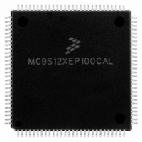
MC9S12XEP100CAL Freescale Semiconductor, MC9S12XEP100CAL Datasheet - Page 645

MC9S12XEP100CAL
Manufacturer Part Number
MC9S12XEP100CAL
Description
IC MCU 16BIT 1M FLASH 112-LQFP
Manufacturer
Freescale Semiconductor
Series
HCS12r
Datasheet
1.MC9S12XEP768CAL.pdf
(1328 pages)
Specifications of MC9S12XEP100CAL
Core Processor
HCS12X
Core Size
16-Bit
Speed
50MHz
Connectivity
CAN, EBI/EMI, I²C, IrDA, SCI, SPI
Peripherals
LVD, POR, PWM, WDT
Number Of I /o
91
Program Memory Size
1MB (1M x 8)
Program Memory Type
FLASH
Eeprom Size
4K x 8
Ram Size
64K x 8
Voltage - Supply (vcc/vdd)
1.72 V ~ 5.5 V
Data Converters
A/D 16x12b
Oscillator Type
External
Operating Temperature
-40°C ~ 85°C
Package / Case
112-LQFP
Processor Series
S12XE
Core
HCS12
Data Bus Width
16 bit
Data Ram Size
64 KB
Interface Type
CAN/SCI/SPI
Maximum Clock Frequency
50 MHz
Number Of Programmable I/os
91
Number Of Timers
25
Maximum Operating Temperature
+ 85 C
Mounting Style
SMD/SMT
3rd Party Development Tools
EWHCS12
Development Tools By Supplier
KIT33812ECUEVME, EVB9S12XEP100, DEMO9S12XEP100
Minimum Operating Temperature
- 40 C
On-chip Adc
16-ch x 12-bit
Package
112LQFP
Family Name
HCS12X
Maximum Speed
50 MHz
Operating Supply Voltage
1.8|2.8|5 V
For Use With
EVB9S12XEP100 - BOARD EVAL FOR MC9S12XEP100DEMO9S12XEP100 - BOARD DEMO FOR MC9S12XEP100
Lead Free Status / RoHS Status
Lead free / RoHS Compliant
Available stocks
Company
Part Number
Manufacturer
Quantity
Price
Company:
Part Number:
MC9S12XEP100CAL
Manufacturer:
TOSHIBA
Quantity:
72
Company:
Part Number:
MC9S12XEP100CAL
Manufacturer:
Freescale Semiconductor
Quantity:
10 000
- Current page: 645 of 1328
- Download datasheet (9Mb)
software simpler because only one address area is applicable for the transmit process, and the required
address space is minimized.
The CPU then stores the identifier, the control bits, and the data content into one of the transmit buffers.
Finally, the buffer is flagged as ready for transmission by clearing the associated TXE flag.
The MSCAN then schedules the message for transmission and signals the successful transmission of the
buffer by setting the associated TXE flag. A transmit interrupt (see
is generated
If more than one buffer is scheduled for transmission when the CAN bus becomes available for arbitration,
the MSCAN uses the local priority setting of the three buffers to determine the prioritization. For this
purpose, every transmit buffer has an 8-bit local priority field (PRIO). The application software programs
this field when the message is set up. The local priority reflects the priority of this particular message
relative to the set of messages being transmitted from this node. The lowest binary value of the PRIO field
is defined to be the highest priority. The internal scheduling process takes place whenever the MSCAN
arbitrates for the CAN bus. This is also the case after the occurrence of a transmission error.
When a high priority message is scheduled by the application software, it may become necessary to abort
a lower priority message in one of the three transmit buffers. Because messages that are already in
transmission cannot be aborted, the user must request the abort by setting the corresponding abort request
bit (ABTRQ) (see
(CANTARQ)”.) The MSCAN then grants the request, if possible, by:
16.4.2.3
The received messages are stored in a five stage input FIFO. The five message buffers are alternately
mapped into a single memory area (see
exclusively associated with the MSCAN, but the foreground receive buffer (RxFG) is addressable by the
CPU (see
applicable for the receive process.
All receive buffers have a size of 15 bytes to store the CAN control bits, the identifier (standard or
extended), the data contents, and a time stamp, if enabled (see
Message
The receiver full flag (RXF) (see
signals the status of the foreground receive buffer. When the buffer contains a correctly received message
with a matching identifier, this flag is set.
On reception, each message is checked to see whether it passes the filter (see
Acceptance
valid message, the MSCAN shifts the content of RxBG into the receiver FIFO, sets the RXF flag, and
1. The transmit interrupt occurs only if not masked. A polling scheme can be applied on TXEx also.
Freescale Semiconductor
1. Setting the corresponding abort acknowledge flag (ABTAK) in the CANTAAK register.
2. Setting the associated TXE flag to release the buffer.
3. Generating a transmit interrupt. The transmit interrupt handler software can determine from the
setting of the ABTAK flag whether the message was aborted (ABTAK = 1) or sent (ABTAK = 0).
Storage”).
Figure
1
Filter”) and simultaneously is written into the active RxBG. After successful reception of a
Receive Structures
when TXEx is set and can be used to drive the application software to re-load the buffer.
16-39). This scheme simplifies the handler software because only one address area is
Section 16.3.2.9, “MSCAN Transmitter Message Abort Request Register
MC9S12XE-Family Reference Manual Rev. 1.23
Section 16.3.2.5, “MSCAN Receiver Flag Register
Figure
16-39). The background receive buffer (RxBG) is
Chapter 16 Freescale’s Scalable Controller Area Network (S12MSCANV3)
Section 16.3.3, “Programmer’s Model of
Section 16.4.7.2, “Transmit
Section 16.4.3, “Identifier
(CANRFLG)”)
Interrupt”)
645
Related parts for MC9S12XEP100CAL
Image
Part Number
Description
Manufacturer
Datasheet
Request
R
Part Number:
Description:
Manufacturer:
Freescale Semiconductor, Inc
Datasheet:
Part Number:
Description:
Manufacturer:
Freescale Semiconductor, Inc
Datasheet:
Part Number:
Description:
Manufacturer:
Freescale Semiconductor, Inc
Datasheet:
Part Number:
Description:
Manufacturer:
Freescale Semiconductor, Inc
Datasheet:
Part Number:
Description:
Manufacturer:
Freescale Semiconductor, Inc
Datasheet:
Part Number:
Description:
Manufacturer:
Freescale Semiconductor, Inc
Datasheet:
Part Number:
Description:
Manufacturer:
Freescale Semiconductor, Inc
Datasheet:
Part Number:
Description:
Manufacturer:
Freescale Semiconductor, Inc
Datasheet:
Part Number:
Description:
Manufacturer:
Freescale Semiconductor, Inc
Datasheet:
Part Number:
Description:
Manufacturer:
Freescale Semiconductor, Inc
Datasheet:
Part Number:
Description:
Manufacturer:
Freescale Semiconductor, Inc
Datasheet:
Part Number:
Description:
Manufacturer:
Freescale Semiconductor, Inc
Datasheet:
Part Number:
Description:
Manufacturer:
Freescale Semiconductor, Inc
Datasheet:
Part Number:
Description:
Manufacturer:
Freescale Semiconductor, Inc
Datasheet:
Part Number:
Description:
Manufacturer:
Freescale Semiconductor, Inc
Datasheet:


