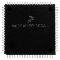
MC9S12XEP100CAL Freescale Semiconductor, MC9S12XEP100CAL Datasheet - Page 894

MC9S12XEP100CAL
Manufacturer Part Number
MC9S12XEP100CAL
Description
IC MCU 16BIT 1M FLASH 112-LQFP
Manufacturer
Freescale Semiconductor
Series
HCS12r
Datasheet
1.MC9S12XEP768CAL.pdf
(1328 pages)
Specifications of MC9S12XEP100CAL
Core Processor
HCS12X
Core Size
16-Bit
Speed
50MHz
Connectivity
CAN, EBI/EMI, I²C, IrDA, SCI, SPI
Peripherals
LVD, POR, PWM, WDT
Number Of I /o
91
Program Memory Size
1MB (1M x 8)
Program Memory Type
FLASH
Eeprom Size
4K x 8
Ram Size
64K x 8
Voltage - Supply (vcc/vdd)
1.72 V ~ 5.5 V
Data Converters
A/D 16x12b
Oscillator Type
External
Operating Temperature
-40°C ~ 85°C
Package / Case
112-LQFP
Processor Series
S12XE
Core
HCS12
Data Bus Width
16 bit
Data Ram Size
64 KB
Interface Type
CAN/SCI/SPI
Maximum Clock Frequency
50 MHz
Number Of Programmable I/os
91
Number Of Timers
25
Maximum Operating Temperature
+ 85 C
Mounting Style
SMD/SMT
3rd Party Development Tools
EWHCS12
Development Tools By Supplier
KIT33812ECUEVME, EVB9S12XEP100, DEMO9S12XEP100
Minimum Operating Temperature
- 40 C
On-chip Adc
16-ch x 12-bit
Package
112LQFP
Family Name
HCS12X
Maximum Speed
50 MHz
Operating Supply Voltage
1.8|2.8|5 V
For Use With
EVB9S12XEP100 - BOARD EVAL FOR MC9S12XEP100DEMO9S12XEP100 - BOARD DEMO FOR MC9S12XEP100
Lead Free Status / RoHS Status
Lead free / RoHS Compliant
Available stocks
Company
Part Number
Manufacturer
Quantity
Price
Company:
Part Number:
MC9S12XEP100CAL
Manufacturer:
TOSHIBA
Quantity:
72
Company:
Part Number:
MC9S12XEP100CAL
Manufacturer:
Freescale Semiconductor
Quantity:
10 000
- Current page: 894 of 1328
- Download datasheet (9Mb)
The Flash memory is ideal for single-supply applications allowing for field reprogramming without
requiring external high voltage sources for program or erase operations. The Flash module includes a
memory controller that executes commands to modify Flash memory contents or configure module
resources for emulated EEPROM operation. The user interface to the memory controller consists of the
indexed Flash Common Command Object (FCCOB) register which is written to with the command, global
address, data, and any required command parameters. The memory controller must complete the execution
of a command before the FCCOB register can be written to with a new command.
The RAM and Flash memory may be read as bytes, aligned words, or misaligned words. Read access time
is one bus cycle for bytes and aligned words, and two bus cycles for misaligned words. For Flash memory,
an erased bit reads 1 and a programmed bit reads 0.
It is not possible to read from a Flash block while any command is executing on that specific Flash block.
It is possible to read from a Flash block while a command is executing on a different Flash block.
Both P-Flash and D-Flash memories are implemented with Error Correction Codes (ECC) that can resolve
single bit faults and detect double bit faults. For P-Flash memory, the ECC implementation requires that
programming be done on an aligned 8 byte basis (a Flash phrase). Since P-Flash memory is always read
by phrase, only one single bit fault in the phrase containing the byte or word accessed will be corrected.
25.1.1
Buffer RAM — The buffer RAM constitutes the volatile memory store required for EEE. Memory space
in the buffer RAM not required for EEE can be partitioned to provide volatile memory space for
applications.
Command Write Sequence — An MCU instruction sequence to execute built-in algorithms (including
program and erase) on the Flash memory.
D-Flash Memory — The D-Flash memory constitutes the nonvolatile memory store required for EEE.
Memory space in the D-Flash memory not required for EEE can be partitioned to provide nonvolatile
memory space for applications.
Freescale Semiconductor
•
•
32 Kbytes of D-Flash (Data Flash) memory, consisting of 1 physical Flash block, that can be used
as nonvolatile storage to support the built-in hardware scheme for emulated EEPROM, as basic
Flash memory primarily intended for nonvolatile data storage, or as a combination of both
4 Kbytes of buffer RAM, consisting of 1 physical RAM block, that can be used as emulated
EEPROM using a built-in hardware scheme, as basic RAM, or as a combination of both
Glossary
A Flash word or phrase must be in the erased state before being
programmed. Cumulative programming of bits within a Flash word or
phrase is not allowed.
MC9S12XE-Family Reference Manual , Rev. 1.23
CAUTION
894
Related parts for MC9S12XEP100CAL
Image
Part Number
Description
Manufacturer
Datasheet
Request
R
Part Number:
Description:
Manufacturer:
Freescale Semiconductor, Inc
Datasheet:
Part Number:
Description:
Manufacturer:
Freescale Semiconductor, Inc
Datasheet:
Part Number:
Description:
Manufacturer:
Freescale Semiconductor, Inc
Datasheet:
Part Number:
Description:
Manufacturer:
Freescale Semiconductor, Inc
Datasheet:
Part Number:
Description:
Manufacturer:
Freescale Semiconductor, Inc
Datasheet:
Part Number:
Description:
Manufacturer:
Freescale Semiconductor, Inc
Datasheet:
Part Number:
Description:
Manufacturer:
Freescale Semiconductor, Inc
Datasheet:
Part Number:
Description:
Manufacturer:
Freescale Semiconductor, Inc
Datasheet:
Part Number:
Description:
Manufacturer:
Freescale Semiconductor, Inc
Datasheet:
Part Number:
Description:
Manufacturer:
Freescale Semiconductor, Inc
Datasheet:
Part Number:
Description:
Manufacturer:
Freescale Semiconductor, Inc
Datasheet:
Part Number:
Description:
Manufacturer:
Freescale Semiconductor, Inc
Datasheet:
Part Number:
Description:
Manufacturer:
Freescale Semiconductor, Inc
Datasheet:
Part Number:
Description:
Manufacturer:
Freescale Semiconductor, Inc
Datasheet:
Part Number:
Description:
Manufacturer:
Freescale Semiconductor, Inc
Datasheet:


