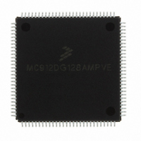
MC912DG128AMPVE Freescale Semiconductor, MC912DG128AMPVE Datasheet - Page 118

MC912DG128AMPVE
Manufacturer Part Number
MC912DG128AMPVE
Description
IC MCU 128K FLASH 8MHZ 112-LQFP
Manufacturer
Freescale Semiconductor
Series
HC12r
Datasheet
1.MC912DG128ACPVER.pdf
(478 pages)
Specifications of MC912DG128AMPVE
Core Processor
CPU12
Core Size
16-Bit
Speed
8MHz
Connectivity
CAN, I²C, SCI, SPI
Peripherals
POR, PWM, WDT
Number Of I /o
69
Program Memory Size
128KB (128K x 8)
Program Memory Type
FLASH
Eeprom Size
2K x 8
Ram Size
8K x 8
Voltage - Supply (vcc/vdd)
4.5 V ~ 5.5 V
Data Converters
A/D 16x8/10b
Oscillator Type
Internal
Operating Temperature
-40°C ~ 125°C
Package / Case
112-LQFP
Processor Series
HC912D
Core
HC12
Data Bus Width
16 bit
Data Ram Size
8 KB
Interface Type
CAN/I2C/SCI/SPI
Maximum Clock Frequency
8 MHz
Number Of Programmable I/os
69
Number Of Timers
8
Maximum Operating Temperature
+ 125 C
Mounting Style
SMD/SMT
3rd Party Development Tools
EWHCS12
Minimum Operating Temperature
- 40 C
On-chip Adc
2 (8-ch x 10-bit)
Lead Free Status / RoHS Status
Lead free / RoHS Compliant
Available stocks
Company
Part Number
Manufacturer
Quantity
Price
Company:
Part Number:
MC912DG128AMPVE
Manufacturer:
FREESCALE
Quantity:
2 902
Company:
Part Number:
MC912DG128AMPVE
Manufacturer:
Freescale Semiconductor
Quantity:
10 000
- Current page: 118 of 478
- Download datasheet (4Mb)
FEECTL — Flash EEPROM Control Register
Flash Memory
Technical Data
118
RESET:
Bit 7
0
0
6
0
0
BOOTP — Boot Protect
FEESWAI — Flash EEPROM Stop in Wait Control
HVEN — High-Voltage Enable
ERAS — Erase Control
The boot blocks are located at $E000–$FFFF and $A000–$BFFF for
odd program pages for each Flash EEPROM module. Since boot
programs must be available at all times, the only useful boot block is
at $E000–$FFFF location. All paged boot blocks can be used as
protected program space if desired.
This register controls the programming and erasure of the Flash
EEPROM.
This bit enables the charge pump to supply high voltages for program
and erase operations in the array. HVEN can only be set if either PGM
or ERAS are set and the proper sequence for program or erase is
followed.
This bit configures the memory for erase operation. ERAS is
interlocked with the PGM bit such that both bits cannot be equal to 1
or set to1 at the same time.
Freescale Semiconductor, Inc.
For More Information On This Product,
0 = Enable erase and program of 8K byte boot block
1 = Disable erase and program of 8K byte boot block
0 = Disables high voltage to array and charge pump off
1 = Enables high voltage to array and charge pump on
0 = Erase operation is not selected.
1 = Erase operation selected.
0 = Do not halt Flash EEPROM clock when the part is in wait
1 = Halt Flash EEPROM clock when the part is in wait mode.
5
0
0
mode.
Go to: www.freescale.com
FEESWAI
Flash Memory
4
0
HVEN
3
0
2
0
0
MC68HC912DT128A — Rev 4.0
ERAS
1
0
PGM
Bit 0
0
MOTOROLA
$00F7
Related parts for MC912DG128AMPVE
Image
Part Number
Description
Manufacturer
Datasheet
Request
R
Part Number:
Description:
Manufacturer:
Freescale Semiconductor, Inc
Datasheet:
Part Number:
Description:
Manufacturer:
Freescale Semiconductor, Inc
Datasheet:
Part Number:
Description:
Manufacturer:
Freescale Semiconductor, Inc
Datasheet:
Part Number:
Description:
Manufacturer:
Freescale Semiconductor, Inc
Datasheet:
Part Number:
Description:
Manufacturer:
Freescale Semiconductor, Inc
Datasheet:
Part Number:
Description:
Manufacturer:
Freescale Semiconductor, Inc
Datasheet:
Part Number:
Description:
Manufacturer:
Freescale Semiconductor, Inc
Datasheet:
Part Number:
Description:
Manufacturer:
Freescale Semiconductor, Inc
Datasheet:
Part Number:
Description:
Manufacturer:
Freescale Semiconductor, Inc
Datasheet:
Part Number:
Description:
Manufacturer:
Freescale Semiconductor, Inc
Datasheet:
Part Number:
Description:
Manufacturer:
Freescale Semiconductor, Inc
Datasheet:
Part Number:
Description:
Manufacturer:
Freescale Semiconductor, Inc
Datasheet:
Part Number:
Description:
Manufacturer:
Freescale Semiconductor, Inc
Datasheet:
Part Number:
Description:
Manufacturer:
Freescale Semiconductor, Inc
Datasheet:
Part Number:
Description:
Manufacturer:
Freescale Semiconductor, Inc
Datasheet:


