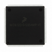
MC912DG128AMPVE Freescale Semiconductor, MC912DG128AMPVE Datasheet - Page 282

MC912DG128AMPVE
Manufacturer Part Number
MC912DG128AMPVE
Description
IC MCU 128K FLASH 8MHZ 112-LQFP
Manufacturer
Freescale Semiconductor
Series
HC12r
Datasheet
1.MC912DG128ACPVER.pdf
(478 pages)
Specifications of MC912DG128AMPVE
Core Processor
CPU12
Core Size
16-Bit
Speed
8MHz
Connectivity
CAN, I²C, SCI, SPI
Peripherals
POR, PWM, WDT
Number Of I /o
69
Program Memory Size
128KB (128K x 8)
Program Memory Type
FLASH
Eeprom Size
2K x 8
Ram Size
8K x 8
Voltage - Supply (vcc/vdd)
4.5 V ~ 5.5 V
Data Converters
A/D 16x8/10b
Oscillator Type
Internal
Operating Temperature
-40°C ~ 125°C
Package / Case
112-LQFP
Processor Series
HC912D
Core
HC12
Data Bus Width
16 bit
Data Ram Size
8 KB
Interface Type
CAN/I2C/SCI/SPI
Maximum Clock Frequency
8 MHz
Number Of Programmable I/os
69
Number Of Timers
8
Maximum Operating Temperature
+ 125 C
Mounting Style
SMD/SMT
3rd Party Development Tools
EWHCS12
Minimum Operating Temperature
- 40 C
On-chip Adc
2 (8-ch x 10-bit)
Lead Free Status / RoHS Status
Lead free / RoHS Compliant
Available stocks
Company
Part Number
Manufacturer
Quantity
Price
Company:
Part Number:
MC912DG128AMPVE
Manufacturer:
FREESCALE
Quantity:
2 902
Company:
Part Number:
MC912DG128AMPVE
Manufacturer:
Freescale Semiconductor
Quantity:
10 000
- Current page: 282 of 478
- Download datasheet (4Mb)
SC0CR1/SC1CR1 — SCI Control Register 1
Multiple Serial Interface
Technical Data
282
RESET:
LOOPS
Bit 7
0
WOMS
6
0
Read or write anytime.
LOOPS — SCI LOOP Mode/Single Wire Mode Enable
WOMS — Wired-Or Mode for Serial Pins
If the DDRS bit associated with the TXD pin is set during the LOOPS
= 1, the TXD pin outputs the SCI waveform. If the DDRS bit
associated with the TXD pin is clear during the LOOPS = 1, the TXD
pin becomes high (IDLE line state) for RSRC = 0 and high impedance
for RSRC = 1. Refer to
This bit controls the two pins (TXD and RXD) associated with the SCIx
section.
Freescale Semiconductor, Inc.
For More Information On This Product,
0 = SCI transmit and receive sections operate normally.
1 = SCI receive section is disconnected from the RXD pin and the
0 = Pins operate in a normal mode with both high and low drive
1 = Each pin operates in an open drain fashion if that pin is
RSRC
5
0
RXD pin is available as general purpose I/O. The receiver input
is determined by the RSRC bit. The transmitter output is
controlled by the associated DDRS bit. Both the transmitter
and the receiver must be enabled to use the LOOP or the
single wire mode.
capability. To affect the RXD bit, that bit would have to be
configured as an output (via DDRS0/2) which is the single wire
case when using the SCI. WOMS bit still affects general-
purpose output on TXD and RXD pins when SCIx is not using
these pins.
declared as an output.
Go to: www.freescale.com
Multiple Serial Interface
M
4
0
WAKE
Table
3
0
16-2.
ILT
2
0
MC68HC912DT128A — Rev 4.0
PE
1
0
Bit 0
PT
0
$00C2/$00CA
MOTOROLA
Related parts for MC912DG128AMPVE
Image
Part Number
Description
Manufacturer
Datasheet
Request
R
Part Number:
Description:
Manufacturer:
Freescale Semiconductor, Inc
Datasheet:
Part Number:
Description:
Manufacturer:
Freescale Semiconductor, Inc
Datasheet:
Part Number:
Description:
Manufacturer:
Freescale Semiconductor, Inc
Datasheet:
Part Number:
Description:
Manufacturer:
Freescale Semiconductor, Inc
Datasheet:
Part Number:
Description:
Manufacturer:
Freescale Semiconductor, Inc
Datasheet:
Part Number:
Description:
Manufacturer:
Freescale Semiconductor, Inc
Datasheet:
Part Number:
Description:
Manufacturer:
Freescale Semiconductor, Inc
Datasheet:
Part Number:
Description:
Manufacturer:
Freescale Semiconductor, Inc
Datasheet:
Part Number:
Description:
Manufacturer:
Freescale Semiconductor, Inc
Datasheet:
Part Number:
Description:
Manufacturer:
Freescale Semiconductor, Inc
Datasheet:
Part Number:
Description:
Manufacturer:
Freescale Semiconductor, Inc
Datasheet:
Part Number:
Description:
Manufacturer:
Freescale Semiconductor, Inc
Datasheet:
Part Number:
Description:
Manufacturer:
Freescale Semiconductor, Inc
Datasheet:
Part Number:
Description:
Manufacturer:
Freescale Semiconductor, Inc
Datasheet:
Part Number:
Description:
Manufacturer:
Freescale Semiconductor, Inc
Datasheet:


