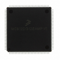
MC912DG128AMPVE Freescale Semiconductor, MC912DG128AMPVE Datasheet - Page 404

MC912DG128AMPVE
Manufacturer Part Number
MC912DG128AMPVE
Description
IC MCU 128K FLASH 8MHZ 112-LQFP
Manufacturer
Freescale Semiconductor
Series
HC12r
Datasheet
1.MC912DG128ACPVER.pdf
(478 pages)
Specifications of MC912DG128AMPVE
Core Processor
CPU12
Core Size
16-Bit
Speed
8MHz
Connectivity
CAN, I²C, SCI, SPI
Peripherals
POR, PWM, WDT
Number Of I /o
69
Program Memory Size
128KB (128K x 8)
Program Memory Type
FLASH
Eeprom Size
2K x 8
Ram Size
8K x 8
Voltage - Supply (vcc/vdd)
4.5 V ~ 5.5 V
Data Converters
A/D 16x8/10b
Oscillator Type
Internal
Operating Temperature
-40°C ~ 125°C
Package / Case
112-LQFP
Processor Series
HC912D
Core
HC12
Data Bus Width
16 bit
Data Ram Size
8 KB
Interface Type
CAN/I2C/SCI/SPI
Maximum Clock Frequency
8 MHz
Number Of Programmable I/os
69
Number Of Timers
8
Maximum Operating Temperature
+ 125 C
Mounting Style
SMD/SMT
3rd Party Development Tools
EWHCS12
Minimum Operating Temperature
- 40 C
On-chip Adc
2 (8-ch x 10-bit)
Lead Free Status / RoHS Status
Lead free / RoHS Compliant
Available stocks
Company
Part Number
Manufacturer
Quantity
Price
Company:
Part Number:
MC912DG128AMPVE
Manufacturer:
FREESCALE
Quantity:
2 902
Company:
Part Number:
MC912DG128AMPVE
Manufacturer:
Freescale Semiconductor
Quantity:
10 000
- Current page: 404 of 478
- Download datasheet (4Mb)
Development Support
20.4.4 BDM Lockout
20.4.4.1 Enabling the BDM lockout
Technical Data
404
complete the requested write operation before a new serial command
disturbs the BDM SHIFTER register.
The external host should delay about 64 target BDMCLK cycles after a
TRACE1 or GO command before starting any new serial command. This
delay is needed because the BDM SHIFTER register is used as a
temporary data holding register during the exit sequence to user code.
BDM logic retains control of the internal buses until a read or write is
completed.If an operation can be completed in a single cycle, it does not
intrude on normal CPU12 operation.However, if an operation requires
multiple cycles, CPU12 clocks are frozen until the operation is complete.
The access to the MCU resources by BDM may be prevented by
enabling the BDM lockout feature. When enabled, the BDM lockout
mechanism prevents the BDM from being active. In this case the BDM
ROM is disabled and does not appear in the MCU memory map.
The BDM lockout is enabled by clearing NOBDML bit of EEMCR
register. The NOBDML bit is loaded at reset from the SHADOW word of
EEPROM module. Modifying the state of the NOBDML and
corresponding EEPROM SHADOW bit is only possible in special modes.
Please refer to
Enabling the BDM lockout feature is only possible in special modes
(SMODN=0) and is accomplished by the following steps.
1. Remove the SHADOW word protection by clearing SHPROT bit in
2. Clear NOSHW bit in EEMCR register to make the SHADOW word
3. Program bit 7 of the high byte of the SHADOW word like a regular
Freescale Semiconductor, Inc.
For More Information On This Product,
EEPROT register.
visible at $0FC0-$0FC1.
EEPROM location at address $0FC0 (write $7F into address
$0FC0). Do not program other bits of the high byte of the
Go to: www.freescale.com
Development Support
EEPROM Memory
for NOBDML information.
MC68HC912DT128A — Rev 4.0
MOTOROLA
Related parts for MC912DG128AMPVE
Image
Part Number
Description
Manufacturer
Datasheet
Request
R
Part Number:
Description:
Manufacturer:
Freescale Semiconductor, Inc
Datasheet:
Part Number:
Description:
Manufacturer:
Freescale Semiconductor, Inc
Datasheet:
Part Number:
Description:
Manufacturer:
Freescale Semiconductor, Inc
Datasheet:
Part Number:
Description:
Manufacturer:
Freescale Semiconductor, Inc
Datasheet:
Part Number:
Description:
Manufacturer:
Freescale Semiconductor, Inc
Datasheet:
Part Number:
Description:
Manufacturer:
Freescale Semiconductor, Inc
Datasheet:
Part Number:
Description:
Manufacturer:
Freescale Semiconductor, Inc
Datasheet:
Part Number:
Description:
Manufacturer:
Freescale Semiconductor, Inc
Datasheet:
Part Number:
Description:
Manufacturer:
Freescale Semiconductor, Inc
Datasheet:
Part Number:
Description:
Manufacturer:
Freescale Semiconductor, Inc
Datasheet:
Part Number:
Description:
Manufacturer:
Freescale Semiconductor, Inc
Datasheet:
Part Number:
Description:
Manufacturer:
Freescale Semiconductor, Inc
Datasheet:
Part Number:
Description:
Manufacturer:
Freescale Semiconductor, Inc
Datasheet:
Part Number:
Description:
Manufacturer:
Freescale Semiconductor, Inc
Datasheet:
Part Number:
Description:
Manufacturer:
Freescale Semiconductor, Inc
Datasheet:


