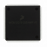
MC912DG128AMPVE Freescale Semiconductor, MC912DG128AMPVE Datasheet - Page 55

MC912DG128AMPVE
Manufacturer Part Number
MC912DG128AMPVE
Description
IC MCU 128K FLASH 8MHZ 112-LQFP
Manufacturer
Freescale Semiconductor
Series
HC12r
Datasheet
1.MC912DG128ACPVER.pdf
(478 pages)
Specifications of MC912DG128AMPVE
Core Processor
CPU12
Core Size
16-Bit
Speed
8MHz
Connectivity
CAN, I²C, SCI, SPI
Peripherals
POR, PWM, WDT
Number Of I /o
69
Program Memory Size
128KB (128K x 8)
Program Memory Type
FLASH
Eeprom Size
2K x 8
Ram Size
8K x 8
Voltage - Supply (vcc/vdd)
4.5 V ~ 5.5 V
Data Converters
A/D 16x8/10b
Oscillator Type
Internal
Operating Temperature
-40°C ~ 125°C
Package / Case
112-LQFP
Processor Series
HC912D
Core
HC12
Data Bus Width
16 bit
Data Ram Size
8 KB
Interface Type
CAN/I2C/SCI/SPI
Maximum Clock Frequency
8 MHz
Number Of Programmable I/os
69
Number Of Timers
8
Maximum Operating Temperature
+ 125 C
Mounting Style
SMD/SMT
3rd Party Development Tools
EWHCS12
Minimum Operating Temperature
- 40 C
On-chip Adc
2 (8-ch x 10-bit)
Lead Free Status / RoHS Status
Lead free / RoHS Compliant
Available stocks
Company
Part Number
Manufacturer
Quantity
Price
Company:
Part Number:
MC912DG128AMPVE
Manufacturer:
FREESCALE
Quantity:
2 902
Company:
Part Number:
MC912DG128AMPVE
Manufacturer:
Freescale Semiconductor
Quantity:
10 000
- Current page: 55 of 478
- Download datasheet (4Mb)
SDO/MOSI
MC68HC912DT128A — Rev 4.0
MOTOROLA
RxCAN2
TxCAN2
Pin Name
SDI/MISO
SMODN/
AN1[7:0]
AN0[7:0]
RxCAN1
RxCAN0
IOC[7:0]
TxCAN1
TxCAN0
PW[3:0]
BKGD/
TAGHI
IX[2:0]
RxD1
RxD0
TEST
XIRQ
TxD1
TxD0
ECS
SCK
SCL
IRQ
SS
(1)
(1)
PAD1[7:0]
PAD0[7:0]
Shared
PK[2:0]
PP[3:0]
PT[7:0]
PIB7
port
PE1
PE0
PK7
PS7
PS6
PS5
PS4
PS2
PS0
PS3
PS1
-
-
-
-
-
-
-
-
Table 3-2. MC68HC912DT128A Signal Description Summary
84/82/80/
78/76/74/
83/81/79/
77/75/73/
112, 1–3 Pulse Width Modulator channel outputs.
Number
109-111 Page Index register emulation outputs.
112-pin
18–15,
72/70
71/69
108
7–4
100
101
102
103
104
105
Pin
55
56
23
96
95
94
93
92
91
90
89
97
98
Freescale Semiconductor, Inc.
For More Information On This Product,
Maskable interrupt request input provides a means of applying asynchronous
Provides a means of requesting asynchronous nonmaskable interrupt requests
During reset, this pin determines special or normal operating mode. After reset,
Emulation Chip select.
Slave select output for SPI master mode, input for slave mode or master mode.
Serial clock for SPI system.
Master out/slave in pin for serial peripheral interface
Master in/slave out pin for serial peripheral interface
SCI1 transmit pin
SCI1 receive pin
SCI0 transmit pin
SCI0 receive pin
Pins used for input capture and output compare in the timer and pulse
Analog inputs for the analog-to-digital conversion module 1
Analog inputs for the analog-to-digital conversion module 0
Used for factory test purposes. Do not connect in the application; may be
MSCAN2 transmit pin (MC68HC912DT128A only). Leave unconnected if
MSCAN2 receive pin (MC68HC912DT128A only). Pin has internal pull-up;
MSCAN1 transmit pin. Leave unconnected if MSCAN1 is not used.
MSCAN1 receive pin. Pin has internal pull-up; where msCAN module is not
MSCAN0 transmit pin. Leave unconnected if MSCAN0 is not used.
MSCAN0 receive pin. Pin has internal pull-up; where msCAN module is not
I
2
interrupt requests to the MCU. Either falling edge-sensitive triggering or level-
sensitive triggering is program selectable (INTCR register).
after reset initialization
single-wire background interface pin is dedicated to the background debug
function. Pin function TAGHI used in instruction tagging. See
Support.
accumulator subsystem.
bonded to 5.5 V max.
MSCAN2 is not used.
where msCAN module is not used, do not tie to VSS.
used, do not tie to VSS.
used, do not tie to VSS.
C bus serial clock line pin
Pinout and Signal Descriptions
Go to: www.freescale.com
Description
Pinout and Signal Descriptions
Signal Descriptions
Development
Technical Data
55
Related parts for MC912DG128AMPVE
Image
Part Number
Description
Manufacturer
Datasheet
Request
R
Part Number:
Description:
Manufacturer:
Freescale Semiconductor, Inc
Datasheet:
Part Number:
Description:
Manufacturer:
Freescale Semiconductor, Inc
Datasheet:
Part Number:
Description:
Manufacturer:
Freescale Semiconductor, Inc
Datasheet:
Part Number:
Description:
Manufacturer:
Freescale Semiconductor, Inc
Datasheet:
Part Number:
Description:
Manufacturer:
Freescale Semiconductor, Inc
Datasheet:
Part Number:
Description:
Manufacturer:
Freescale Semiconductor, Inc
Datasheet:
Part Number:
Description:
Manufacturer:
Freescale Semiconductor, Inc
Datasheet:
Part Number:
Description:
Manufacturer:
Freescale Semiconductor, Inc
Datasheet:
Part Number:
Description:
Manufacturer:
Freescale Semiconductor, Inc
Datasheet:
Part Number:
Description:
Manufacturer:
Freescale Semiconductor, Inc
Datasheet:
Part Number:
Description:
Manufacturer:
Freescale Semiconductor, Inc
Datasheet:
Part Number:
Description:
Manufacturer:
Freescale Semiconductor, Inc
Datasheet:
Part Number:
Description:
Manufacturer:
Freescale Semiconductor, Inc
Datasheet:
Part Number:
Description:
Manufacturer:
Freescale Semiconductor, Inc
Datasheet:
Part Number:
Description:
Manufacturer:
Freescale Semiconductor, Inc
Datasheet:


