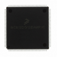
MC912DG128AMPVE Freescale Semiconductor, MC912DG128AMPVE Datasheet - Page 62

MC912DG128AMPVE
Manufacturer Part Number
MC912DG128AMPVE
Description
IC MCU 128K FLASH 8MHZ 112-LQFP
Manufacturer
Freescale Semiconductor
Series
HC12r
Datasheet
1.MC912DG128ACPVER.pdf
(478 pages)
Specifications of MC912DG128AMPVE
Core Processor
CPU12
Core Size
16-Bit
Speed
8MHz
Connectivity
CAN, I²C, SCI, SPI
Peripherals
POR, PWM, WDT
Number Of I /o
69
Program Memory Size
128KB (128K x 8)
Program Memory Type
FLASH
Eeprom Size
2K x 8
Ram Size
8K x 8
Voltage - Supply (vcc/vdd)
4.5 V ~ 5.5 V
Data Converters
A/D 16x8/10b
Oscillator Type
Internal
Operating Temperature
-40°C ~ 125°C
Package / Case
112-LQFP
Processor Series
HC912D
Core
HC12
Data Bus Width
16 bit
Data Ram Size
8 KB
Interface Type
CAN/I2C/SCI/SPI
Maximum Clock Frequency
8 MHz
Number Of Programmable I/os
69
Number Of Timers
8
Maximum Operating Temperature
+ 125 C
Mounting Style
SMD/SMT
3rd Party Development Tools
EWHCS12
Minimum Operating Temperature
- 40 C
On-chip Adc
2 (8-ch x 10-bit)
Lead Free Status / RoHS Status
Lead free / RoHS Compliant
Available stocks
Company
Part Number
Manufacturer
Quantity
Price
Company:
Part Number:
MC912DG128AMPVE
Manufacturer:
FREESCALE
Quantity:
2 902
Company:
Part Number:
MC912DG128AMPVE
Manufacturer:
Freescale Semiconductor
Quantity:
10 000
- Current page: 62 of 478
- Download datasheet (4Mb)
Pinout and Signal Descriptions
3.5.11 Port AD1
3.5.12 Port AD0
3.5.13 Port P
Technical Data
62
This port is an analog input interface to the analog-to-digital subsystem
and used for general-purpose input. When analog-to-digital functions
are not enabled, the port has eight general-purpose input pins,
PAD1[7:0]. The ADPU bit in the ATD1CTL2 register enables the A/D
function.
Port AD1 pins are inputs; no data direction register is associated with this
port. The port has no resistive input loads and no reduced drive controls.
Refer to
This port is an analog input interface to the analog-to-digital subsystem
and used for general-purpose input. When analog-to-digital functions
are not enabled, the port has eight general-purpose input pins,
PAD0[7:0]. The ADPU bit in the ATD0CTL2 register enables the A/D
function.
Port AD0 pins are inputs; no data direction register is associated with this
port. The port has no resistive input loads and no reduced drive controls.
Refer to
The four pulse-width modulation channel outputs share general-purpose
port P pins. The PWM function is enabled with the PWEN register.
Enabling PWM pins takes precedence over the general-purpose port.
When pulse-width modulation is not in use, the port pins may be used for
general-purpose I/O.
Register DDRP determines pin direction of port P when used for
general-purpose I/O. When DDRP bits are set, the corresponding pin is
configured for output. On reset the DDRP bits are cleared and the
corresponding pin is configured for input.
When the PUPP bit in the PWCTL register is set, all input pins are pulled
up internally by an active pull-up device. Pullups are disabled after reset.
Freescale Semiconductor, Inc.
For More Information On This Product,
Analog-to-Digital
Analog-to-Digital
Pinout and Signal Descriptions
Go to: www.freescale.com
Converter.
Converter.
MC68HC912DT128A — Rev 4.0
MOTOROLA
Related parts for MC912DG128AMPVE
Image
Part Number
Description
Manufacturer
Datasheet
Request
R
Part Number:
Description:
Manufacturer:
Freescale Semiconductor, Inc
Datasheet:
Part Number:
Description:
Manufacturer:
Freescale Semiconductor, Inc
Datasheet:
Part Number:
Description:
Manufacturer:
Freescale Semiconductor, Inc
Datasheet:
Part Number:
Description:
Manufacturer:
Freescale Semiconductor, Inc
Datasheet:
Part Number:
Description:
Manufacturer:
Freescale Semiconductor, Inc
Datasheet:
Part Number:
Description:
Manufacturer:
Freescale Semiconductor, Inc
Datasheet:
Part Number:
Description:
Manufacturer:
Freescale Semiconductor, Inc
Datasheet:
Part Number:
Description:
Manufacturer:
Freescale Semiconductor, Inc
Datasheet:
Part Number:
Description:
Manufacturer:
Freescale Semiconductor, Inc
Datasheet:
Part Number:
Description:
Manufacturer:
Freescale Semiconductor, Inc
Datasheet:
Part Number:
Description:
Manufacturer:
Freescale Semiconductor, Inc
Datasheet:
Part Number:
Description:
Manufacturer:
Freescale Semiconductor, Inc
Datasheet:
Part Number:
Description:
Manufacturer:
Freescale Semiconductor, Inc
Datasheet:
Part Number:
Description:
Manufacturer:
Freescale Semiconductor, Inc
Datasheet:
Part Number:
Description:
Manufacturer:
Freescale Semiconductor, Inc
Datasheet:


