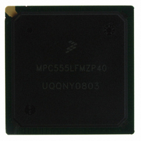
MPC555LFMZP40 Freescale Semiconductor, MPC555LFMZP40 Datasheet - Page 177

MPC555LFMZP40
Manufacturer Part Number
MPC555LFMZP40
Description
IC MCU 32BIT 40MHZ 272-BGA
Manufacturer
Freescale Semiconductor
Series
MPC5xxr
Datasheets
1.MPC555LFMZP40.pdf
(12 pages)
2.MPC555LFMZP40.pdf
(966 pages)
3.MPC555LFMZP40.pdf
(3 pages)
Specifications of MPC555LFMZP40
Core Processor
PowerPC
Core Size
32-Bit
Speed
40MHz
Connectivity
CAN, EBI/EMI, SCI, SPI, UART/USART
Peripherals
POR, PWM, WDT
Number Of I /o
101
Program Memory Size
448KB (448K x 8)
Program Memory Type
FLASH
Ram Size
26K x 8
Voltage - Supply (vcc/vdd)
2.5 V ~ 2.7 V
Data Converters
A/D 32x10b
Oscillator Type
External
Operating Temperature
-40°C ~ 125°C
Package / Case
272-PBGA
Controller Family/series
POWER 5xx
Ram Memory Size
26KB
Cpu Speed
63MIPS
Embedded Interface Type
QSPI, SCI, TouCAN
Operating Temperature Range
-40°C To +125°C
No. Of Pins
272
Rohs Compliant
No
Processor Series
MPC5xx
Core
PowerPC
Data Bus Width
32 bit
Data Ram Size
26 KB
Interface Type
CAN, QSPI, SCI
Maximum Clock Frequency
40 MHz
Number Of Programmable I/os
101
Operating Supply Voltage
3.3 V to 5 V
Maximum Operating Temperature
+ 125 C
Mounting Style
SMD/SMT
Development Tools By Supplier
MPC555CMEE
Minimum Operating Temperature
- 85 C
On-chip Adc
10 bit, 32 Channel
Cpu Family
MPC55xx
Device Core
PowerPC
Device Core Size
32b
Frequency (max)
40MHz
Total Internal Ram Size
32KB
# I/os (max)
101
Operating Supply Voltage (typ)
5V
Instruction Set Architecture
RISC
Operating Temp Range
-40C to 85C
Operating Temperature Classification
Industrial
Mounting
Surface Mount
Pin Count
272
Package Type
BGA
For Use With
MPC555CMEE - KIT EVAL FOR MPC555
Lead Free Status / RoHS Status
Contains lead / RoHS non-compliant
Eeprom Size
-
Lead Free Status / Rohs Status
No
Available stocks
Company
Part Number
Manufacturer
Quantity
Price
Company:
Part Number:
MPC555LFMZP40
Manufacturer:
MOTOLOLA
Quantity:
853
Company:
Part Number:
MPC555LFMZP40
Manufacturer:
Freescale Semiconductor
Quantity:
10 000
Company:
Part Number:
MPC555LFMZP40R2
Manufacturer:
Freescale Semiconductor
Quantity:
10 000
- Current page: 177 of 966
- Download datasheet (15Mb)
4.1 Burst Buffer Block Diagram
MPC555 / MPC556
USER’S MANUAL
The burst buffer module consists of the burst buffer controller (BBC) and the instruc-
tion memory protection unit (IMPU).
The BBC delivers the RCPU instruction fetch accesses from the instruction bus onto
the U-bus. It utilizes the full U-bus pipeline and a special page access attribute in order
to take full advantage of the U-bus bandwidth. It can handle both burstable and non-
burstable external memories as well as non-burstable internal memories (flash EE-
PROM, SRAM).
Code compression features are only available on the MPC556. The MPC556 utilizes
a version of code compression / decompression which is called “Phase A”. Phase A
code compression / decompression is described in this manual. Future parts may have
a different type of code compression. The BBC also contains the functional module
which is called the instruction code decompressor unit (ICDU). The ICDU is responsi-
ble for on-line (previously compressed) instruction code decompression in the “De-
compression-ON” mode. In the “Decompression-OFF” mode, the ICDU is bypassed
and the BBC is in normal function.
The IMPU allows the memory to be divided into four regions with different attributes,
as well as a default global region (for memory space that is not included in either of the
two regions). Each of the two regions can be of size four Kbytes to four Gbytes. Over-
lap between regions is allowed.
The IMPU includes registers that contain the following information: region base ad-
dress, region size and the region’s access permissions. For each access (from the
processor to the memory), the IMPU finds which region matches the address. If more
than one region matches, the region with the lowest index is chosen. If no region is
matched, the global region is chosen.
The IMPU compares the attributes of the access from the processor to the attributes
of the appropriate region. If the access is allowed, the proper signals are sent to the
BBC. If the access is not permitted, an interrupt is sent to the processor.
The IMPU does not support address translation. The effective fetch address issued by
the processor is the one that is transferred to the U-bus.
Figure 4-1
is a block diagram of the burst buffer.
Freescale Semiconductor, Inc.
For More Information On This Product,
Go to: www.freescale.com
BURST BUFFER
Rev. 15 October 2000
BURST BUFFER
SECTION 4
MOTOROLA
4-1
Related parts for MPC555LFMZP40
Image
Part Number
Description
Manufacturer
Datasheet
Request
R
Part Number:
Description:
Manufacturer:
Freescale Semiconductor, Inc
Datasheet:
Part Number:
Description:
Manufacturer:
Freescale Semiconductor, Inc
Datasheet:
Part Number:
Description:
Manufacturer:
Freescale Semiconductor, Inc
Datasheet:
Part Number:
Description:
Manufacturer:
Freescale Semiconductor, Inc
Datasheet:
Part Number:
Description:
Manufacturer:
Freescale Semiconductor, Inc
Datasheet:
Part Number:
Description:
Manufacturer:
Freescale Semiconductor, Inc
Datasheet:
Part Number:
Description:
Manufacturer:
Freescale Semiconductor, Inc
Datasheet:
Part Number:
Description:
Manufacturer:
Freescale Semiconductor, Inc
Datasheet:
Part Number:
Description:
Manufacturer:
Freescale Semiconductor, Inc
Datasheet:
Part Number:
Description:
Manufacturer:
Freescale Semiconductor, Inc
Datasheet:
Part Number:
Description:
Manufacturer:
Freescale Semiconductor, Inc
Datasheet:
Part Number:
Description:
Manufacturer:
Freescale Semiconductor, Inc
Datasheet:
Part Number:
Description:
Manufacturer:
Freescale Semiconductor, Inc
Datasheet:
Part Number:
Description:
Manufacturer:
Freescale Semiconductor, Inc
Datasheet:
Part Number:
Description:
Manufacturer:
Freescale Semiconductor, Inc
Datasheet:


