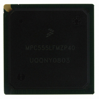
MPC555LFMZP40 Freescale Semiconductor, MPC555LFMZP40 Datasheet - Page 520

MPC555LFMZP40
Manufacturer Part Number
MPC555LFMZP40
Description
IC MCU 32BIT 40MHZ 272-BGA
Manufacturer
Freescale Semiconductor
Series
MPC5xxr
Datasheets
1.MPC555LFMZP40.pdf
(12 pages)
2.MPC555LFMZP40.pdf
(966 pages)
3.MPC555LFMZP40.pdf
(3 pages)
Specifications of MPC555LFMZP40
Core Processor
PowerPC
Core Size
32-Bit
Speed
40MHz
Connectivity
CAN, EBI/EMI, SCI, SPI, UART/USART
Peripherals
POR, PWM, WDT
Number Of I /o
101
Program Memory Size
448KB (448K x 8)
Program Memory Type
FLASH
Ram Size
26K x 8
Voltage - Supply (vcc/vdd)
2.5 V ~ 2.7 V
Data Converters
A/D 32x10b
Oscillator Type
External
Operating Temperature
-40°C ~ 125°C
Package / Case
272-PBGA
Controller Family/series
POWER 5xx
Ram Memory Size
26KB
Cpu Speed
63MIPS
Embedded Interface Type
QSPI, SCI, TouCAN
Operating Temperature Range
-40°C To +125°C
No. Of Pins
272
Rohs Compliant
No
Processor Series
MPC5xx
Core
PowerPC
Data Bus Width
32 bit
Data Ram Size
26 KB
Interface Type
CAN, QSPI, SCI
Maximum Clock Frequency
40 MHz
Number Of Programmable I/os
101
Operating Supply Voltage
3.3 V to 5 V
Maximum Operating Temperature
+ 125 C
Mounting Style
SMD/SMT
Development Tools By Supplier
MPC555CMEE
Minimum Operating Temperature
- 85 C
On-chip Adc
10 bit, 32 Channel
Cpu Family
MPC55xx
Device Core
PowerPC
Device Core Size
32b
Frequency (max)
40MHz
Total Internal Ram Size
32KB
# I/os (max)
101
Operating Supply Voltage (typ)
5V
Instruction Set Architecture
RISC
Operating Temp Range
-40C to 85C
Operating Temperature Classification
Industrial
Mounting
Surface Mount
Pin Count
272
Package Type
BGA
For Use With
MPC555CMEE - KIT EVAL FOR MPC555
Lead Free Status / RoHS Status
Contains lead / RoHS non-compliant
Eeprom Size
-
Lead Free Status / Rohs Status
No
Available stocks
Company
Part Number
Manufacturer
Quantity
Price
Company:
Part Number:
MPC555LFMZP40
Manufacturer:
MOTOLOLA
Quantity:
853
Company:
Part Number:
MPC555LFMZP40
Manufacturer:
Freescale Semiconductor
Quantity:
10 000
Company:
Part Number:
MPC555LFMZP40R2
Manufacturer:
Freescale Semiconductor
Quantity:
10 000
- Current page: 520 of 966
- Download datasheet (15Mb)
14.8.7.9 Receiver Wake-Up
14.8.7.10 Internal Loop Mode
14.9 SCI Queue Operation
14.9.1 Queue Operation of SCI1 for Transmit and Receive
MPC555
USER’S MANUAL
The receiver wake-up function allows a transmitting device to direct a transmission to
a single receiver or to a group of receivers by sending an address frame at the start of
a message. Hardware activates each receiver in a system under certain conditions.
Resident software must process address information and enable or disable receiver
operation.
A receiver is placed in wake-up mode by setting the RWU bit in SCCxR1. While RWU
is set, receiver status flags and interrupts are disabled. Although the software can
clear RWU, it is normally cleared by hardware during wake-up.
The WAKE bit in SCCxR1 determines which type of wake-up is used. When WAKE =
0, idle-line wake-up is selected. When WAKE = 1, address-mark wake-up is selected.
Both types require a software-based device addressing and recognition scheme.
Idle-line wake-up allows a receiver to sleep until an idle line is detected. When an idle
line is detected, the receiver clears RWU and wakes up. The receiver waits for the first
frame of the next transmission. The data frame is received normally, transferred to the
RDRx, and the RDRF flag is set. If software does not recognize the address, it can set
RWU and put the receiver back to sleep. For idle-line wake-up to work, there must be
a minimum of one frame of idle line between transmissions. There must be no idle time
between frames within a transmission.
Address mark wake-up uses a special frame format to wake up the receiver. When the
MSB of an address-mark frame is set, that frame contains address information. The
first frame of each transmission must be an address frame. When the MSB of a frame
is set, the receiver clears RWU and wakes up. The data frame is received normally,
transferred to the RDRx, and the RDRF flag is set. If software does not recognize the
address, it can set RWU and put the receiver back to sleep. Address mark wake-up
allows idle time between frames and eliminates idle time between transmissions. How-
ever, there is a loss of efficiency because of an additional bit-time per frame.
The LOOPS bit in SCCxR1 controls a feedback path in the data serial shifter. When
LOOPS is set, the SCI transmitter output is fed back into the receive serial shifter. TXD
is asserted (idle line). Both transmitter and receiver must be enabled before entering
loop mode.
The SCI1 serial module allows for queueing on transmit and receive data frames. In
the standard mode, in which the queue is disabled, the SCI1 operates as previously
defined (i.e. transmit and receive operations done via SC1DR). However, if the SCI1
queue feature is enabled (by setting the QTE and/or QRE bits within QSCI1CR) a set
of 16 entry queues is allocated for the receive and/or transmit operation. Through soft-
/
MPC556
Freescale Semiconductor, Inc.
QUEUED SERIAL MULTI-CHANNEL MODULE
For More Information On This Product,
Go to: www.freescale.com
Rev. 15 October 2000
MOTOROLA
14-58
Related parts for MPC555LFMZP40
Image
Part Number
Description
Manufacturer
Datasheet
Request
R
Part Number:
Description:
Manufacturer:
Freescale Semiconductor, Inc
Datasheet:
Part Number:
Description:
Manufacturer:
Freescale Semiconductor, Inc
Datasheet:
Part Number:
Description:
Manufacturer:
Freescale Semiconductor, Inc
Datasheet:
Part Number:
Description:
Manufacturer:
Freescale Semiconductor, Inc
Datasheet:
Part Number:
Description:
Manufacturer:
Freescale Semiconductor, Inc
Datasheet:
Part Number:
Description:
Manufacturer:
Freescale Semiconductor, Inc
Datasheet:
Part Number:
Description:
Manufacturer:
Freescale Semiconductor, Inc
Datasheet:
Part Number:
Description:
Manufacturer:
Freescale Semiconductor, Inc
Datasheet:
Part Number:
Description:
Manufacturer:
Freescale Semiconductor, Inc
Datasheet:
Part Number:
Description:
Manufacturer:
Freescale Semiconductor, Inc
Datasheet:
Part Number:
Description:
Manufacturer:
Freescale Semiconductor, Inc
Datasheet:
Part Number:
Description:
Manufacturer:
Freescale Semiconductor, Inc
Datasheet:
Part Number:
Description:
Manufacturer:
Freescale Semiconductor, Inc
Datasheet:
Part Number:
Description:
Manufacturer:
Freescale Semiconductor, Inc
Datasheet:
Part Number:
Description:
Manufacturer:
Freescale Semiconductor, Inc
Datasheet:


