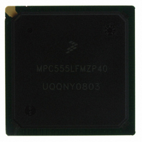
MPC555LFMZP40 Freescale Semiconductor, MPC555LFMZP40 Datasheet - Page 589

MPC555LFMZP40
Manufacturer Part Number
MPC555LFMZP40
Description
IC MCU 32BIT 40MHZ 272-BGA
Manufacturer
Freescale Semiconductor
Series
MPC5xxr
Datasheets
1.MPC555LFMZP40.pdf
(12 pages)
2.MPC555LFMZP40.pdf
(966 pages)
3.MPC555LFMZP40.pdf
(3 pages)
Specifications of MPC555LFMZP40
Core Processor
PowerPC
Core Size
32-Bit
Speed
40MHz
Connectivity
CAN, EBI/EMI, SCI, SPI, UART/USART
Peripherals
POR, PWM, WDT
Number Of I /o
101
Program Memory Size
448KB (448K x 8)
Program Memory Type
FLASH
Ram Size
26K x 8
Voltage - Supply (vcc/vdd)
2.5 V ~ 2.7 V
Data Converters
A/D 32x10b
Oscillator Type
External
Operating Temperature
-40°C ~ 125°C
Package / Case
272-PBGA
Controller Family/series
POWER 5xx
Ram Memory Size
26KB
Cpu Speed
63MIPS
Embedded Interface Type
QSPI, SCI, TouCAN
Operating Temperature Range
-40°C To +125°C
No. Of Pins
272
Rohs Compliant
No
Processor Series
MPC5xx
Core
PowerPC
Data Bus Width
32 bit
Data Ram Size
26 KB
Interface Type
CAN, QSPI, SCI
Maximum Clock Frequency
40 MHz
Number Of Programmable I/os
101
Operating Supply Voltage
3.3 V to 5 V
Maximum Operating Temperature
+ 125 C
Mounting Style
SMD/SMT
Development Tools By Supplier
MPC555CMEE
Minimum Operating Temperature
- 85 C
On-chip Adc
10 bit, 32 Channel
Cpu Family
MPC55xx
Device Core
PowerPC
Device Core Size
32b
Frequency (max)
40MHz
Total Internal Ram Size
32KB
# I/os (max)
101
Operating Supply Voltage (typ)
5V
Instruction Set Architecture
RISC
Operating Temp Range
-40C to 85C
Operating Temperature Classification
Industrial
Mounting
Surface Mount
Pin Count
272
Package Type
BGA
For Use With
MPC555CMEE - KIT EVAL FOR MPC555
Lead Free Status / RoHS Status
Contains lead / RoHS non-compliant
Eeprom Size
-
Lead Free Status / Rohs Status
No
Available stocks
Company
Part Number
Manufacturer
Quantity
Price
Company:
Part Number:
MPC555LFMZP40
Manufacturer:
MOTOLOLA
Quantity:
853
Company:
Part Number:
MPC555LFMZP40
Manufacturer:
Freescale Semiconductor
Quantity:
10 000
Company:
Part Number:
MPC555LFMZP40R2
Manufacturer:
Freescale Semiconductor
Quantity:
10 000
- Current page: 589 of 966
- Download datasheet (15Mb)
16.3.1.5 Message Buffer Activation/Deactivation Mechanism
16.3.1.6 Message Buffer Lock/Release/Busy Mechanism
16.3.2 Receive Mask Registers
MPC555
USER’S MANUAL
Each message buffer must be activated once the user configures it for the desired op-
eration. A buffer is activated by writing the appropriate code to the control/status word
for that buffer. Once the buffer is activated, it will begin participating in the normal
transmit and receive processes.
A buffer is deactivated by writing the appropriate deactivation code to the control/sta-
tus word for that buffer. A buffer is typically deactivated when the user desires to re-
configure the buffer (for example to change the buffer’s function from Rx to Tx or Tx to
Rx). The buffer should also be deactivated before changing a receive buffer’s mes-
sage identifier or before loading a new message to be transmitted into a transmit buff-
er.
For more details on activation and deactivation of message buffers and the effects on
message buffer operation, refer to
In addition to the activation/deactivation mechanism, the TouCAN also uses a lock/re-
lease/busy mechanism to ensure data coherency during the receive process. The
mechanism includes a lock status for each message buffer and uses the two serial
message buffers to facilitate frame transfers within the TouCAN.
Reading the control/status word of a receive message buffer triggers the lock for that
buffer. While locked, a received message cannot be transferred into that buffer from
one of the serial message buffers.
If a message transfer between the message buffer and a serial message buffer is in
progress when the control/status word is read, the BUSY status is indicated in the
code field, and the lock is not activated.
The user can release the lock on a message buffer in one of two ways. Reading the
control/status word of another message buffer locks that buffer, releasing the previ-
ously locked buffer. A global release can also be performed on any locked message
buffer by reading the free-running timer.
Once a lock is released, any message transfers between a serial message buffer and
a message buffer that were delayed due to that buffer being locked will take place. For
more details on the message buffer locking mechanism, and the effects on message
buffer operation, refer to
The receive mask registers are used as acceptance masks for received frame IDs.
The following masks are defined:
The value of the mask registers should not be changed during normal operation. If the
mask register data is changed after the masked identifier of a received message is
• A global mask, used for receive buffers 0-13
• Two separate masks for buffers 14 and 15
/
MPC556
Freescale Semiconductor, Inc.
For More Information On This Product,
16.4 TouCAN
CAN 2.0B CONTROLLER MODULE
Go to: www.freescale.com
Rev. 15 October 2000
16.4 TouCAN
Operation.
Operation.
MOTOROLA
16-7
Related parts for MPC555LFMZP40
Image
Part Number
Description
Manufacturer
Datasheet
Request
R
Part Number:
Description:
Manufacturer:
Freescale Semiconductor, Inc
Datasheet:
Part Number:
Description:
Manufacturer:
Freescale Semiconductor, Inc
Datasheet:
Part Number:
Description:
Manufacturer:
Freescale Semiconductor, Inc
Datasheet:
Part Number:
Description:
Manufacturer:
Freescale Semiconductor, Inc
Datasheet:
Part Number:
Description:
Manufacturer:
Freescale Semiconductor, Inc
Datasheet:
Part Number:
Description:
Manufacturer:
Freescale Semiconductor, Inc
Datasheet:
Part Number:
Description:
Manufacturer:
Freescale Semiconductor, Inc
Datasheet:
Part Number:
Description:
Manufacturer:
Freescale Semiconductor, Inc
Datasheet:
Part Number:
Description:
Manufacturer:
Freescale Semiconductor, Inc
Datasheet:
Part Number:
Description:
Manufacturer:
Freescale Semiconductor, Inc
Datasheet:
Part Number:
Description:
Manufacturer:
Freescale Semiconductor, Inc
Datasheet:
Part Number:
Description:
Manufacturer:
Freescale Semiconductor, Inc
Datasheet:
Part Number:
Description:
Manufacturer:
Freescale Semiconductor, Inc
Datasheet:
Part Number:
Description:
Manufacturer:
Freescale Semiconductor, Inc
Datasheet:
Part Number:
Description:
Manufacturer:
Freescale Semiconductor, Inc
Datasheet:


