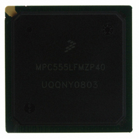
MPC555LFMZP40 Freescale Semiconductor, MPC555LFMZP40 Datasheet - Page 680

MPC555LFMZP40
Manufacturer Part Number
MPC555LFMZP40
Description
IC MCU 32BIT 40MHZ 272-BGA
Manufacturer
Freescale Semiconductor
Series
MPC5xxr
Datasheets
1.MPC555LFMZP40.pdf
(12 pages)
2.MPC555LFMZP40.pdf
(966 pages)
3.MPC555LFMZP40.pdf
(3 pages)
Specifications of MPC555LFMZP40
Core Processor
PowerPC
Core Size
32-Bit
Speed
40MHz
Connectivity
CAN, EBI/EMI, SCI, SPI, UART/USART
Peripherals
POR, PWM, WDT
Number Of I /o
101
Program Memory Size
448KB (448K x 8)
Program Memory Type
FLASH
Ram Size
26K x 8
Voltage - Supply (vcc/vdd)
2.5 V ~ 2.7 V
Data Converters
A/D 32x10b
Oscillator Type
External
Operating Temperature
-40°C ~ 125°C
Package / Case
272-PBGA
Controller Family/series
POWER 5xx
Ram Memory Size
26KB
Cpu Speed
63MIPS
Embedded Interface Type
QSPI, SCI, TouCAN
Operating Temperature Range
-40°C To +125°C
No. Of Pins
272
Rohs Compliant
No
Processor Series
MPC5xx
Core
PowerPC
Data Bus Width
32 bit
Data Ram Size
26 KB
Interface Type
CAN, QSPI, SCI
Maximum Clock Frequency
40 MHz
Number Of Programmable I/os
101
Operating Supply Voltage
3.3 V to 5 V
Maximum Operating Temperature
+ 125 C
Mounting Style
SMD/SMT
Development Tools By Supplier
MPC555CMEE
Minimum Operating Temperature
- 85 C
On-chip Adc
10 bit, 32 Channel
Cpu Family
MPC55xx
Device Core
PowerPC
Device Core Size
32b
Frequency (max)
40MHz
Total Internal Ram Size
32KB
# I/os (max)
101
Operating Supply Voltage (typ)
5V
Instruction Set Architecture
RISC
Operating Temp Range
-40C to 85C
Operating Temperature Classification
Industrial
Mounting
Surface Mount
Pin Count
272
Package Type
BGA
For Use With
MPC555CMEE - KIT EVAL FOR MPC555
Lead Free Status / RoHS Status
Contains lead / RoHS non-compliant
Eeprom Size
-
Lead Free Status / Rohs Status
No
Available stocks
Company
Part Number
Manufacturer
Quantity
Price
Company:
Part Number:
MPC555LFMZP40
Manufacturer:
MOTOLOLA
Quantity:
853
Company:
Part Number:
MPC555LFMZP40
Manufacturer:
Freescale Semiconductor
Quantity:
10 000
Company:
Part Number:
MPC555LFMZP40R2
Manufacturer:
Freescale Semiconductor
Quantity:
10 000
- Current page: 680 of 966
- Download datasheet (15Mb)
19.7.3 System Clock Scaling
MPC555
USER’S MANUAL
The following subsections explain how the values for R, N, and M are determined.
The first term of the pulse width timing equation is the clock scaling, R. The value of R
is determined by the system clock range (SCLKR) field. SCLKR defines the pulse tim-
er’s base clock using the system clock. Use
the system clock frequency. The system clock period is multiplied by the clock scaling
value to generate a 83.3-ns to 125-ns scaled clock. This scaled clock is used to run
the charge pump submodule and the next functional block of the timing control.
SCLKR[0:2]
110 and 111
/
MPC556
000
001
010
011
100
101
Where:
The minimum specified system clock frequency for performing pro-
gram and erase operations is 8.0 MHz. The CMF EEPROM does not
have any means to monitor the system clock frequency and will not
prevent program or erase operation at frequencies below 8.0 MHz.
Attempting to program or erase the CMF EEPROM at system clock
frequencies lower than 8.0 MHz will not damage the device if the
maximum pulse times and total times are not exceeded. While some
bits in the CMF EEPROM array may change state if programmed or
erased at system clock frequencies below 8.0 MHz, the full program
or erase transition is not ensured.
Never stop the U-bus clock or alter its frequency during a program or
erase operation. Changing the clock frequency during a program or
erase operation results in inaccurate pulse widths and variations in
the charge pump output. This includes loss of system clock/PLL.
R = Clock Scaling
N = 5 + CLKPE[0:1] + ((PE | CSC)
M = 1 + CLKPM[0:6]
Not for customer use.
not specified and pulse is not terminated by the timer con-
Freescale Semiconductor, Inc.
Pulse Width = System Clock Period
For More Information On This Product,
trol. Recovery time is specified to be 128 clocks.
Table 19-12 System Clock Range
Minimum
CDR MoneT FLASH EEPROM
System Clock Frequency (MHz)
12
18
24
36
8
Go to: www.freescale.com
Rev. 15 October 2000
Program and erase timing control
Reserved by Motorola for future use
WARNING
NOTE
Table 19-12
Maximum
12
18
24
36
40
•
10)
•
R
to set SCLKR based upon
•
2
N
•
M
Clock Scaling (R)
3/2
1
1
2
3
4
MOTOROLA
19-28
Related parts for MPC555LFMZP40
Image
Part Number
Description
Manufacturer
Datasheet
Request
R
Part Number:
Description:
Manufacturer:
Freescale Semiconductor, Inc
Datasheet:
Part Number:
Description:
Manufacturer:
Freescale Semiconductor, Inc
Datasheet:
Part Number:
Description:
Manufacturer:
Freescale Semiconductor, Inc
Datasheet:
Part Number:
Description:
Manufacturer:
Freescale Semiconductor, Inc
Datasheet:
Part Number:
Description:
Manufacturer:
Freescale Semiconductor, Inc
Datasheet:
Part Number:
Description:
Manufacturer:
Freescale Semiconductor, Inc
Datasheet:
Part Number:
Description:
Manufacturer:
Freescale Semiconductor, Inc
Datasheet:
Part Number:
Description:
Manufacturer:
Freescale Semiconductor, Inc
Datasheet:
Part Number:
Description:
Manufacturer:
Freescale Semiconductor, Inc
Datasheet:
Part Number:
Description:
Manufacturer:
Freescale Semiconductor, Inc
Datasheet:
Part Number:
Description:
Manufacturer:
Freescale Semiconductor, Inc
Datasheet:
Part Number:
Description:
Manufacturer:
Freescale Semiconductor, Inc
Datasheet:
Part Number:
Description:
Manufacturer:
Freescale Semiconductor, Inc
Datasheet:
Part Number:
Description:
Manufacturer:
Freescale Semiconductor, Inc
Datasheet:
Part Number:
Description:
Manufacturer:
Freescale Semiconductor, Inc
Datasheet:


