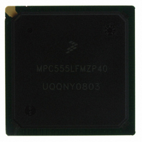
MPC555LFMZP40 Freescale Semiconductor, MPC555LFMZP40 Datasheet - Page 760

MPC555LFMZP40
Manufacturer Part Number
MPC555LFMZP40
Description
IC MCU 32BIT 40MHZ 272-BGA
Manufacturer
Freescale Semiconductor
Series
MPC5xxr
Datasheets
1.MPC555LFMZP40.pdf
(12 pages)
2.MPC555LFMZP40.pdf
(966 pages)
3.MPC555LFMZP40.pdf
(3 pages)
Specifications of MPC555LFMZP40
Core Processor
PowerPC
Core Size
32-Bit
Speed
40MHz
Connectivity
CAN, EBI/EMI, SCI, SPI, UART/USART
Peripherals
POR, PWM, WDT
Number Of I /o
101
Program Memory Size
448KB (448K x 8)
Program Memory Type
FLASH
Ram Size
26K x 8
Voltage - Supply (vcc/vdd)
2.5 V ~ 2.7 V
Data Converters
A/D 32x10b
Oscillator Type
External
Operating Temperature
-40°C ~ 125°C
Package / Case
272-PBGA
Controller Family/series
POWER 5xx
Ram Memory Size
26KB
Cpu Speed
63MIPS
Embedded Interface Type
QSPI, SCI, TouCAN
Operating Temperature Range
-40°C To +125°C
No. Of Pins
272
Rohs Compliant
No
Processor Series
MPC5xx
Core
PowerPC
Data Bus Width
32 bit
Data Ram Size
26 KB
Interface Type
CAN, QSPI, SCI
Maximum Clock Frequency
40 MHz
Number Of Programmable I/os
101
Operating Supply Voltage
3.3 V to 5 V
Maximum Operating Temperature
+ 125 C
Mounting Style
SMD/SMT
Development Tools By Supplier
MPC555CMEE
Minimum Operating Temperature
- 85 C
On-chip Adc
10 bit, 32 Channel
Cpu Family
MPC55xx
Device Core
PowerPC
Device Core Size
32b
Frequency (max)
40MHz
Total Internal Ram Size
32KB
# I/os (max)
101
Operating Supply Voltage (typ)
5V
Instruction Set Architecture
RISC
Operating Temp Range
-40C to 85C
Operating Temperature Classification
Industrial
Mounting
Surface Mount
Pin Count
272
Package Type
BGA
For Use With
MPC555CMEE - KIT EVAL FOR MPC555
Lead Free Status / RoHS Status
Contains lead / RoHS non-compliant
Eeprom Size
-
Lead Free Status / Rohs Status
No
Available stocks
Company
Part Number
Manufacturer
Quantity
Price
Company:
Part Number:
MPC555LFMZP40
Manufacturer:
MOTOLOLA
Quantity:
853
Company:
Part Number:
MPC555LFMZP40
Manufacturer:
Freescale Semiconductor
Quantity:
10 000
Company:
Part Number:
MPC555LFMZP40R2
Manufacturer:
Freescale Semiconductor
Quantity:
10 000
- Current page: 760 of 966
- Download datasheet (15Mb)
22.5.4 CLAMP
22.5.5 HI-Z
22.6 Restrictions
22.7 Low-Power Stop Mode
MPC555
USER’S MANUAL
When the bypass register is selected by the current instruction, the shift register stage
is set to a logic zero on the rising edge of TCK in the capture-DR controller state.
Therefore, the first bit to be shifted out after selecting the bypass register will always
be a logic zero.
The CLAMP instruction selects the single-bit bypass register as shown in
4, and the state of all signals driven from system output pins is completely defined by
the data previously shifted into the boundary scan register (e.g., using the SAMPLE/
PRELOAD instruction).
The HI-Z instruction is provided as a manufacturer’s optional public instruction to pre-
vent having to backdrive the output pins during circuit-board testing. When HI-Z is in-
voked, all output drivers, including the two-state drivers, are turned off (i.e., high
impedance). The instruction selects the bypass register.
The MPC555 / MPC556 provides flexible control of external signals using the bound-
ary scan register and EXTEST or CLAMP instructions. As a result, the circuit board
test environment must be designed to avoid signal contention which may result in de-
vice destruction.
The MPC555 / MPC556 features a low-power stop mode. The interaction of the scan
chain interface with low-power stop mode is as follows:
1. The TAP controller must be in the test-logic-reset state to either enter or remain
/
MPC556
in the low-power stop mode. Leaving the TAP controller in the test-logic-reset
state negates the ability to achieve low-power, but does not otherwise affect de-
vice functionality.
FROM TDI
SHIFT DR
Freescale Semiconductor, Inc.
IEEE 1149.1-COMPLIANT INTERFACE (JTAG)
0
For More Information On This Product,
Figure 22-4 Bypass Register
Go to: www.freescale.com
Rev. 15 October 2000
G1
1
1
MUX
CLOCK DR
D
C
TO TDO
Figure 22-
MOTOROLA
22-6
Related parts for MPC555LFMZP40
Image
Part Number
Description
Manufacturer
Datasheet
Request
R
Part Number:
Description:
Manufacturer:
Freescale Semiconductor, Inc
Datasheet:
Part Number:
Description:
Manufacturer:
Freescale Semiconductor, Inc
Datasheet:
Part Number:
Description:
Manufacturer:
Freescale Semiconductor, Inc
Datasheet:
Part Number:
Description:
Manufacturer:
Freescale Semiconductor, Inc
Datasheet:
Part Number:
Description:
Manufacturer:
Freescale Semiconductor, Inc
Datasheet:
Part Number:
Description:
Manufacturer:
Freescale Semiconductor, Inc
Datasheet:
Part Number:
Description:
Manufacturer:
Freescale Semiconductor, Inc
Datasheet:
Part Number:
Description:
Manufacturer:
Freescale Semiconductor, Inc
Datasheet:
Part Number:
Description:
Manufacturer:
Freescale Semiconductor, Inc
Datasheet:
Part Number:
Description:
Manufacturer:
Freescale Semiconductor, Inc
Datasheet:
Part Number:
Description:
Manufacturer:
Freescale Semiconductor, Inc
Datasheet:
Part Number:
Description:
Manufacturer:
Freescale Semiconductor, Inc
Datasheet:
Part Number:
Description:
Manufacturer:
Freescale Semiconductor, Inc
Datasheet:
Part Number:
Description:
Manufacturer:
Freescale Semiconductor, Inc
Datasheet:
Part Number:
Description:
Manufacturer:
Freescale Semiconductor, Inc
Datasheet:


