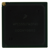
MPC555LFMZP40 Freescale Semiconductor, MPC555LFMZP40 Datasheet - Page 864

MPC555LFMZP40
Manufacturer Part Number
MPC555LFMZP40
Description
IC MCU 32BIT 40MHZ 272-BGA
Manufacturer
Freescale Semiconductor
Series
MPC5xxr
Datasheets
1.MPC555LFMZP40.pdf
(12 pages)
2.MPC555LFMZP40.pdf
(966 pages)
3.MPC555LFMZP40.pdf
(3 pages)
Specifications of MPC555LFMZP40
Core Processor
PowerPC
Core Size
32-Bit
Speed
40MHz
Connectivity
CAN, EBI/EMI, SCI, SPI, UART/USART
Peripherals
POR, PWM, WDT
Number Of I /o
101
Program Memory Size
448KB (448K x 8)
Program Memory Type
FLASH
Ram Size
26K x 8
Voltage - Supply (vcc/vdd)
2.5 V ~ 2.7 V
Data Converters
A/D 32x10b
Oscillator Type
External
Operating Temperature
-40°C ~ 125°C
Package / Case
272-PBGA
Controller Family/series
POWER 5xx
Ram Memory Size
26KB
Cpu Speed
63MIPS
Embedded Interface Type
QSPI, SCI, TouCAN
Operating Temperature Range
-40°C To +125°C
No. Of Pins
272
Rohs Compliant
No
Processor Series
MPC5xx
Core
PowerPC
Data Bus Width
32 bit
Data Ram Size
26 KB
Interface Type
CAN, QSPI, SCI
Maximum Clock Frequency
40 MHz
Number Of Programmable I/os
101
Operating Supply Voltage
3.3 V to 5 V
Maximum Operating Temperature
+ 125 C
Mounting Style
SMD/SMT
Development Tools By Supplier
MPC555CMEE
Minimum Operating Temperature
- 85 C
On-chip Adc
10 bit, 32 Channel
Cpu Family
MPC55xx
Device Core
PowerPC
Device Core Size
32b
Frequency (max)
40MHz
Total Internal Ram Size
32KB
# I/os (max)
101
Operating Supply Voltage (typ)
5V
Instruction Set Architecture
RISC
Operating Temp Range
-40C to 85C
Operating Temperature Classification
Industrial
Mounting
Surface Mount
Pin Count
272
Package Type
BGA
For Use With
MPC555CMEE - KIT EVAL FOR MPC555
Lead Free Status / RoHS Status
Contains lead / RoHS non-compliant
Eeprom Size
-
Lead Free Status / Rohs Status
No
Available stocks
Company
Part Number
Manufacturer
Quantity
Price
Company:
Part Number:
MPC555LFMZP40
Manufacturer:
MOTOLOLA
Quantity:
853
Company:
Part Number:
MPC555LFMZP40
Manufacturer:
Freescale Semiconductor
Quantity:
10 000
Company:
Part Number:
MPC555LFMZP40R2
Manufacturer:
Freescale Semiconductor
Quantity:
10 000
- Current page: 864 of 966
- Download datasheet (15Mb)
D.19.1.1 CHAN_CONTROL
D.19.1.2 BIT_D
D.19.1.3 HALF_PERIOD
D.19.1.4 BIT_COUNT
D.19.1.5 XFER_SIZE
D.19.1.6 SIOP_DATA
MPC555 / MPC556
USER’S MANUAL
NOTES:
This 9-bit CPU written parameter is used to setup the clock polarity for the SIOP data
transfer. The valid values for CHAN_CONTROL for this function are given in the table
below. CHAN_CONTROL must be written by the host prior to issuing the host service
request (HSR) to initialize the function.
1. Other values of CHAN_CONTROL may result in indeterminate operation.
BIT_D is a CPU written bit that determines the direction of shift of the SIOP data. If
BIT_D is zero then SIOP_DATA is right shifted (lsb first). If BIT_D is one then
SIOP_DATA is left shifted (msb first).
This CPU-written parameter defines the baud rate of the SIOP function. The value
contained in HALF_PERIOD is the number of TCR1 counts for a half SIOP clock pe-
riod (e.g., for a 50 KHz baud rate, with a TCR1 period of 240 ns, the value [(1/50 KHz)/
2]/240 ns = 42 should be written to HALF_PERIOD. The range for HALF_PERIOD is
1 to 0x8000, although the minimum value in practice will be limited by other system
conditions. See notes on use and performance of SIOP function.
This parameter is used by the TPU to count down the number bits remaining while a
transfer is in progress. During the SIOP initialization state, BIT_COUNT is loaded with
the value contained in XFER_SIZE. It is then decremented as the data is transferred
and when it reaches zero, the transfer is complete and the TPU issues an interrupt re-
quest to the CPU.
This CPU-written parameter determines the number of bits that make up a data trans-
fer. During initialization, XFER_SIZE is copied into BIT_COUNT. XFER_SIZE is
shown as a 5-bit parameter to match the maximum size of 16 bits in SIOP_DATA, al-
though the TPU uses the whole word location. For normal use, XFER_SIZE should
be in the range 1-to-16.
This parameter is the data register for all SIOP transfers. Data is shifted out of one
end of SIOP_DATA and shifted in at the other end, the shift direction being determined
CHAN_CONTROL
8 7 6 5 4 3 2 1 0
0 1 0 0 0 1 1 0 1
0 1 0 0 0 1 1 1 0
Table D-4 SIOP Function Valid CHAN_Control Options
Freescale Semiconductor, Inc.
1
For More Information On This Product,
Go to: www.freescale.com
TPU ROM FUNCTIONS
Rev. 15 October 2000
Data valid on clock Falling edge.
Data valid on clock Rising edge.
Resulting Action
MOTOROLA
D-50
Related parts for MPC555LFMZP40
Image
Part Number
Description
Manufacturer
Datasheet
Request
R
Part Number:
Description:
Manufacturer:
Freescale Semiconductor, Inc
Datasheet:
Part Number:
Description:
Manufacturer:
Freescale Semiconductor, Inc
Datasheet:
Part Number:
Description:
Manufacturer:
Freescale Semiconductor, Inc
Datasheet:
Part Number:
Description:
Manufacturer:
Freescale Semiconductor, Inc
Datasheet:
Part Number:
Description:
Manufacturer:
Freescale Semiconductor, Inc
Datasheet:
Part Number:
Description:
Manufacturer:
Freescale Semiconductor, Inc
Datasheet:
Part Number:
Description:
Manufacturer:
Freescale Semiconductor, Inc
Datasheet:
Part Number:
Description:
Manufacturer:
Freescale Semiconductor, Inc
Datasheet:
Part Number:
Description:
Manufacturer:
Freescale Semiconductor, Inc
Datasheet:
Part Number:
Description:
Manufacturer:
Freescale Semiconductor, Inc
Datasheet:
Part Number:
Description:
Manufacturer:
Freescale Semiconductor, Inc
Datasheet:
Part Number:
Description:
Manufacturer:
Freescale Semiconductor, Inc
Datasheet:
Part Number:
Description:
Manufacturer:
Freescale Semiconductor, Inc
Datasheet:
Part Number:
Description:
Manufacturer:
Freescale Semiconductor, Inc
Datasheet:
Part Number:
Description:
Manufacturer:
Freescale Semiconductor, Inc
Datasheet:


