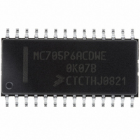
MC705P6ACDWE Freescale Semiconductor, MC705P6ACDWE Datasheet - Page 42

MC705P6ACDWE
Manufacturer Part Number
MC705P6ACDWE
Description
IC MCU 176 BYTES RAM 28-SOIC
Manufacturer
Freescale Semiconductor
Series
HC05r
Datasheet
1.MC705P6ACDWE.pdf
(98 pages)
Specifications of MC705P6ACDWE
Core Processor
HC05
Core Size
8-Bit
Speed
2.1MHz
Connectivity
SIO
Peripherals
POR, WDT
Number Of I /o
21
Program Memory Size
4.5KB (4.5K x 8)
Program Memory Type
OTP
Ram Size
176 x 8
Voltage - Supply (vcc/vdd)
3 V ~ 5.5 V
Data Converters
A/D 4x8b
Oscillator Type
Internal
Operating Temperature
-40°C ~ 85°C
Package / Case
28-SOIC (7.5mm Width)
Processor Series
HC705P
Core
HC05
Data Bus Width
8 bit
Data Ram Size
176 B
Maximum Clock Frequency
2.1 MHz
Number Of Programmable I/os
21
Number Of Timers
1
Maximum Operating Temperature
+ 85 C
Mounting Style
SMD/SMT
Minimum Operating Temperature
- 40 C
On-chip Adc
8 bit, 4 Channel
Lead Free Status / RoHS Status
Lead free / RoHS Compliant
Eeprom Size
-
Lead Free Status / Rohs Status
Details
Available stocks
Company
Part Number
Manufacturer
Quantity
Price
Company:
Part Number:
MC705P6ACDWE
Manufacturer:
Freescale Semiconductor
Quantity:
135
Part Number:
MC705P6ACDWE
Manufacturer:
FREESCALE
Quantity:
20 000
Serial Input/Output Port (SIOP)
7.2 SIOP Signal Format
The SIOP subsystem is software configurable for master or slave operation. No external mode selection
inputs are available (for instance, slave select pin).
7.2.1 Serial Clock (SCK)
The state of the SCK output normally remains a logic 1 during idle periods between data transfers. The
first falling edge of SCK signals the beginning of a data transfer. At this time, the first bit of received data
may be presented at the SDI pin and the first bit of transmitted data is presented at the SDO pin (see
Figure
the eighth rising edge of SCK.
The master and slave modes of operation differ only by the sourcing of SCK. In master mode, SCK is
driven from an internal source within the MCU. In slave mode, SCK is driven from a source external to the
MCU. The SCK frequency is dependent upon the SPR0 and SPR1 bits located in the mask option
register. Refer to
7.2.2 Serial Data Input (SDI)
The SDI pin becomes an input as soon as the SIOP subsystem is enabled. New data may be presented
to the SDI pin on the falling edge of SCK.However, valid data must be present at least 100 nanoseconds
before the rising edge of SCK and remain valid for 100 nanoseconds after the rising edge of SCK. See
Figure
7.2.3 Serial Data Output (SDO)
The SDO pin becomes an output as soon as the SIOP subsystem is enabled. Prior to enabling the SIOP,
PB5 can be initialized to determine the beginning state. While the SIOP is enabled, PB5 cannot be used
as a standard output since that pin is connected to the last stage of the SIOP serial shift register. Mask
option register bit LSBF permits data to be transmitted in either the MSB first format or the LSB first format.
Refer to
On the first falling edge of SCK, the first data bit will be shifted out to the SDO pin. The remaining data
bits will be shifted out to the SDO pin on subsequent falling edges of SCK. The SDO pin will present valid
data at least 100 nanoseconds before the rising edge of the SCK and remain valid for 100 nanoseconds
after the rising edge of SCK. See
42
SDO
SCK
SDI
7-2). Data is captured at the SDI pin on the rising edge of SCK. The transfer is terminated upon
7-2.
11.2 Mask Option Register
11.2 Mask Option Register
BIT 0
BIT 0
MC68HC705P6A Advance Information Data Sheet, Rev. 2.1
100 ns
BIT 1
BIT 1
Figure
Figure 7-2. SIOP Timing Diagram
for MOR LSBF programming information.
BIT 2
BIT 2
7-2.
for a description of available SCK frequencies.
BIT 3
BIT 3
BIT 4
BIT 4
BIT 5
BIT 5
100 ns
BIT 6
BIT 6
Freescale Semiconductor
BIT 7
BIT 7


