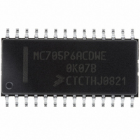
MC705P6ACDWE Freescale Semiconductor, MC705P6ACDWE Datasheet - Page 55

MC705P6ACDWE
Manufacturer Part Number
MC705P6ACDWE
Description
IC MCU 176 BYTES RAM 28-SOIC
Manufacturer
Freescale Semiconductor
Series
HC05r
Datasheet
1.MC705P6ACDWE.pdf
(98 pages)
Specifications of MC705P6ACDWE
Core Processor
HC05
Core Size
8-Bit
Speed
2.1MHz
Connectivity
SIO
Peripherals
POR, WDT
Number Of I /o
21
Program Memory Size
4.5KB (4.5K x 8)
Program Memory Type
OTP
Ram Size
176 x 8
Voltage - Supply (vcc/vdd)
3 V ~ 5.5 V
Data Converters
A/D 4x8b
Oscillator Type
Internal
Operating Temperature
-40°C ~ 85°C
Package / Case
28-SOIC (7.5mm Width)
Processor Series
HC705P
Core
HC05
Data Bus Width
8 bit
Data Ram Size
176 B
Maximum Clock Frequency
2.1 MHz
Number Of Programmable I/os
21
Number Of Timers
1
Maximum Operating Temperature
+ 85 C
Mounting Style
SMD/SMT
Minimum Operating Temperature
- 40 C
On-chip Adc
8 bit, 4 Channel
Lead Free Status / RoHS Status
Lead free / RoHS Compliant
Eeprom Size
-
Lead Free Status / Rohs Status
Details
Available stocks
Company
Part Number
Manufacturer
Quantity
Price
Company:
Part Number:
MC705P6ACDWE
Manufacturer:
Freescale Semiconductor
Quantity:
135
Part Number:
MC705P6ACDWE
Manufacturer:
FREESCALE
Quantity:
20 000
ADRC — RC Oscillator Control
ADON — A/D Subsystem On
CH2–CH0 — Channel Select Bits
9.6 A/D Conversion Data Register (ADC)
This register contains the output of the A/D converter. See
Freescale Semiconductor
When ADRC is set, the A/D subsystem operates from the internal RC oscillator instead of the internal
clock. The RC oscillator requires a time, t
obtained. See
When the A/D subsystem is turned on (ADON = 1), it requires a time, t
accurate conversion results can be attained.
CH2, CH1, and CH0 form a 3-bit field which is used to select an input to the A/D converter. Channels
0–3 correspond to port C input pins PC6–PC3. Channels 4–6 are used for reference measurements.
Channel 7 is reserved. If a conversion is attempted with channel 7 selected, the result will be $00.
Table 9-1
If the ADON bit is set and an input from channels 0–4 is selected, the corresponding port C pin’s DDR
bit will be cleared (making that port C pin an input). If the port C data register is read while the A/D is
on and one of the shared input channels is selected using bit CH0–CH2, the corresponding port C pin
will read as a logic 0. The remaining port C pins will read normally. To digitally read a port C pin, the
A/D subsystem must be disabled (ADON = 0), or input channels 5–7 must be selected.
lists the inputs selected by bits CH0-CH3.
Address: $001D
Reset:
Read:
Write:
9.2.2 Reference Voltage (VREFH)
Figure 9-2. A/D Conversion Value Data Register (ADC)
Table 9-1. A/D Multiplexer Input Channel Assignments
Bit 7
AD7
MC68HC705P6A Advance Information Data Sheet, Rev. 2.1
= Unimplemented
AD6
Channel
6
0
1
2
3
4
5
6
7
AD5
5
RCON
, to stabilize before accurate conversion results can be
Unaffected by reset
AD4
4
for more information.
Reserved for factory test
V
AD0 — port C, bit 6
AD1 — port C, bit 5
AD2 — port C, bit 4
AD3 — port C, bit 3
Figure
REFH
AD3
(V
3
REFH
— port C, bit 7
Signal
V
9-2.
SS
+ V
AD2
SS
2
)/2
A/D Conversion Data Register (ADC)
ADON
AD1
1
, to stabilize before
Bit 0
AD0
55


