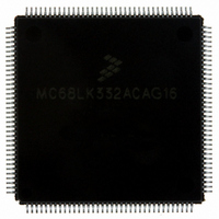
MC68LK332ACAG16 Freescale Semiconductor, MC68LK332ACAG16 Datasheet - Page 11

MC68LK332ACAG16
Manufacturer Part Number
MC68LK332ACAG16
Description
IC MCU 32BIT LV AMASK 144-LQFP
Manufacturer
Freescale Semiconductor
Series
M683xxr
Specifications of MC68LK332ACAG16
Core Processor
CPU32
Core Size
32-Bit
Speed
16.78MHz
Connectivity
EBI/EMI, SCI, SPI, UART/USART
Peripherals
POR, PWM, WDT
Number Of I /o
15
Program Memory Type
ROMless
Ram Size
2K x 8
Voltage - Supply (vcc/vdd)
3 V ~ 3.6 V
Oscillator Type
Internal
Operating Temperature
-40°C ~ 85°C
Package / Case
144-LQFP
Processor Series
M683xx
Core
CPU32
Data Bus Width
32 bit
Maximum Clock Frequency
16 MHz
Maximum Operating Temperature
+ 85 C
Mounting Style
SMD/SMT
Interface Type
QSPI, SCI, UART
Minimum Operating Temperature
- 40 C
No. Of I/o's
15
Ram Memory Size
2KB
Cpu Speed
16MHz
No. Of Timers
16
Embedded Interface Type
QSPI, SCI, UART
Digital Ic Case Style
LQFP
Rohs Compliant
Yes
Data Ram Size
2 KB
Number Of Programmable I/os
15
Number Of Timers
16
Cpu Family
68K/M683xx
Device Core
ColdFire
Device Core Size
32b
Frequency (max)
16MHz
Program Memory Size
Not Required
Total Internal Ram Size
2KB
# I/os (max)
15
Number Of Timers - General Purpose
16
Operating Supply Voltage (typ)
5V
Instruction Set Architecture
RISC
Operating Temp Range
-40C to 85C
Operating Temperature Classification
Industrial
Mounting
Surface Mount
Pin Count
144
Package Type
LQFP
Lead Free Status / RoHS Status
Lead free / RoHS Compliant
Eeprom Size
-
Program Memory Size
-
Data Converters
-
Lead Free Status / Rohs Status
Lead free / RoHS Compliant
Available stocks
Company
Part Number
Manufacturer
Quantity
Price
Company:
Part Number:
MC68LK332ACAG16
Manufacturer:
MOTOLOLA
Quantity:
1 045
Company:
Part Number:
MC68LK332ACAG16
Manufacturer:
Freescale Semiconductor
Quantity:
10 000
Part Number:
MC68LK332ACAG16
Manufacturer:
FREESCALE
Quantity:
20 000
MC68LK332
MC68CK331EC16/D
Num
NOTES:
10. After external RESET negation is detected, a short transition period (approximately 2) t
11. External assertion of the RESET input can overlap internally-generated resets. To insure that an external reset
12. External logic must pull RESET high during this period in order for normal MCU operation to begin.
77
78
1. All AC timing is shown with respect to 2.0 V to 0.8 V levels unless otherwise noted.
2. When an external clock is used, minimum high and low times are based on a 50% duty cycle. The minimum
3. Specification 9A is the worst-case skew between AS and DS or CS. The amount of skew depends on the relative
4. If multiple chip-selects are used, CS width negated (specification 15) applies to the time from the negation of a
5. Hold times are specified with respect to DS or CS on asynchronous reads and with respect to CLKOUT on fast
6. Maximum value is equal to (t
7. If the asynchronous setup time (specification 47A) requirements are satisfied, the DSACK[1:0] low to data setup
8. To ensure coherency during every operand transfer, BG is not asserted in response to BR until after all cycles
9. In the absence of DSACK[1:0], BERR is an asynchronous input using the asynchronous setup time (specification
drives RESET low for 512 t
is recognized in all cases, RESET must be asserted for at least 590 CLKOUT cycles.
allowable t
external clock input duty cycle and minimum t
loading of these signals. When loads are kept within specified limits, skew will not cause AS and DS to fall outside
the limits shown in specification 9.
heavily loaded chip-select to the assertion of a lightly loaded chip select. The CS width negated specification
between multiple chip-selects does not apply to chip selects being used for synchronous ECLK cycles.
cycle reads. The user is free to use either hold time.
time (specification 31) and DSACK[1:0] low to BERR low setup time (specification 48) can be ignored. The data
must only satisfy the data-in to clock low setup time (specification 27) for the following clock cycle. BERR must
satisfy only the late BERR low to clock low setup time (specification 27A) for the following clock cycle.
of the current operand transfer are complete.
47A).
RESET Assertion Time
RESET Rise Time
Xcyc
Minimum t
period is reduced when the duty cycle of the external clock varies. The relationship between
(V
DD
11, 12
and V
Freescale Semiconductor, Inc.
Xcyc
10
cyc
For More Information On This Product,
Table 6 16.78 MHz AC Timing (Continued)
cyc
.
DDSYN
Characteristic
period = minimum t
/ 2) + 25 ns.
= 3.0 to 3.6 Vdc, V
Go to: www.freescale.com
Xcyc
XCHL
is expressed:
/ (50% – external clock input duty cycle tolerance).
SS
= 0 Vdc, T
A
= T
Symbol
t
t
RSTR
RSTA
L
to T
H
1
cyc
Min
elapses, then the SIM
—
4
MOTOROLA
Max
10
—
Unit
t
t
cyc
cyc
11


