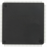
DF70845AD80FPV Renesas Electronics America, DF70845AD80FPV Datasheet - Page 30

DF70845AD80FPV
Manufacturer Part Number
DF70845AD80FPV
Description
IC SUPERH MCU FLASH 112LQFP
Manufacturer
Renesas Electronics America
Series
SuperH® SH7080r
Datasheet
1.DF70844AD80FPV.pdf
(1644 pages)
Specifications of DF70845AD80FPV
Core Size
32-Bit
Program Memory Size
512KB (512K x 8)
Core Processor
SH-2
Speed
80MHz
Connectivity
EBI/EMI, FIFO, I²C, SCI, SSU
Peripherals
DMA, POR, PWM, WDT
Number Of I /o
76
Program Memory Type
FLASH
Ram Size
32K x 8
Voltage - Supply (vcc/vdd)
3 V ~ 5.5 V
Data Converters
A/D 8x10b
Oscillator Type
Internal
Operating Temperature
-40°C ~ 85°C
Package / Case
112-LQFP
No. Of I/o's
76
Ram Memory Size
32KB
Cpu Speed
80MHz
Digital Ic Case Style
LQFP
Supply Voltage Range
3V To 3.6V, 4.5V To 5.5V
Embedded Interface Type
I2C, SCI
Rohs Compliant
Yes
Lead Free Status / RoHS Status
Lead free / RoHS Compliant
For Use With
R0K570865S001BE - KIT STARTER FOR SH7086R0K570865S000BE - KIT STARTER FOR SH7086HS0005KCU11H - EMULATOR E10A-USB H8S(X),SH2(A)
Eeprom Size
-
Lead Free Status / RoHS Status
Lead free / RoHS Compliant, Lead free / RoHS Compliant
Available stocks
Company
Part Number
Manufacturer
Quantity
Price
Company:
Part Number:
DF70845AD80FPV
Manufacturer:
TAIYO
Quantity:
40 000
Company:
Part Number:
DF70845AD80FPV
Manufacturer:
Renesas Electronics America
Quantity:
10 000
- Current page: 30 of 1644
- Download datasheet (10Mb)
Figure 9.14 Example of 32-Bit Data Width SDRAM Connection
Figure 9.15 Example of 16-Bit Data Width SDRAM Connection
Figure 9.16 Example of 16-Bit Data Width SDRAM Connection
Figure 9.17 Burst Read Basic Timing (Auto-Precharge)............................................................ 318
Figure 9.18 Burst Read Wait Specification Timing (Auto-Precharge)....................................... 319
Figure 9.19 Single Read Basic Timing (Auto-Precharge) .......................................................... 320
Figure 9.20 Basic Timing for SDRAM Burst Write (Auto-Precharge) ...................................... 322
Figure 9.21 Single Write Basic Timing (Auto-Precharge) ......................................................... 323
Figure 9.22 Burst Read Timing (No Auto-Precharge)................................................................ 325
Figure 9.23 Burst Read Timing (Bank Active, Same Row Address) ......................................... 326
Figure 9.24 Burst Read Timing (Bank Active, Different Row Addresses) ................................ 327
Figure 9.25 Single Write Timing (No Auto-Precharge) ............................................................. 328
Figure 9.26 Single Write Timing (Bank Active, Same Row Address)....................................... 329
Figure 9.27 Single Write Timing (Bank Active, Different Row Addresses).............................. 330
Figure 9.28 Auto-Refresh Timing .............................................................................................. 332
Figure 9.29 Self-Refresh Timing ................................................................................................ 333
Figure 9.30 SDRAM Mode Register Write Timing (Based on JEDEC) .................................... 336
Figure 9.31 Burst ROM (Clock Asynchronous) Access
Figure 9.32 Basic Access Timing for SRAM with Byte Selection (BAS = 0) ........................... 340
Figure 9.33 Basic Access Timing for SRAM with Byte Selection (BAS = 1) ........................... 341
Figure 9.34 Byte Selection SRAM Wait Timing
Figure 9.35 Example of Connection with 32-Bit Data Width Byte-Selection SRAM................ 343
Figure 9.36 Example of Connection with 16-Bit Data Width Byte-Selection SRAM................ 343
Figure 9.37 Example of PCMCIA Interface Connection............................................................ 345
Figure 9.38 Basic Access Timing for PCMCIA Memory Card Interface................................... 346
Figure 9.39 Wait Timing for PCMCIA Memory Card Interface
Figure 9.40 Example of PCMCIA Space Assignment
Figure 9.41 Basic Timing for PCMCIA I/O Card Interface ....................................................... 349
Figure 9.42 Wait Timing for PCMCIA I/O Card Interface Timing
Figure 9.43 Burst MPX Device Connection Example................................................................ 351
Figure 9.44 Burst MPX Space Access Timing (Single Read, No Wait or Software Wait 1) ..... 352
Rev. 3.00 May 17, 2007 Page xxx of Iviii
(RASU and CASU are not Used) ............................................................................ 302
(RASU and CASU are not Used) ............................................................................ 303
(RASU and CASU are Used) .................................................................................. 304
(Bus Width = 32 Bits, 16 byte Transfer (Number of Burst = 4),
Access Wait for the 1st time = 2, Access Wait for 2nd Time and after = 1) ........... 339
(BAS = 1, SW[1:0] = 01, WR[3:0] = 0001, HW[1:0] = 01).................................... 342
(TED[3:0] = B'0010, TEH[3:0] = B'0001, Hardware Wait = 1).............................. 347
(CS5WCR.SA[1:0] = B'10, CS6WCR.SA[1:0] = B'10).......................................... 348
(TED[3:0] = B'0010, TEH[3:0] = B'0001, Hardware Wait 1) ................................. 350
Related parts for DF70845AD80FPV
Image
Part Number
Description
Manufacturer
Datasheet
Request
R

Part Number:
Description:
KIT STARTER FOR M16C/29
Manufacturer:
Renesas Electronics America
Datasheet:

Part Number:
Description:
KIT STARTER FOR R8C/2D
Manufacturer:
Renesas Electronics America
Datasheet:

Part Number:
Description:
R0K33062P STARTER KIT
Manufacturer:
Renesas Electronics America
Datasheet:

Part Number:
Description:
KIT STARTER FOR R8C/23 E8A
Manufacturer:
Renesas Electronics America
Datasheet:

Part Number:
Description:
KIT STARTER FOR R8C/25
Manufacturer:
Renesas Electronics America
Datasheet:

Part Number:
Description:
KIT STARTER H8S2456 SHARPE DSPLY
Manufacturer:
Renesas Electronics America
Datasheet:

Part Number:
Description:
KIT STARTER FOR R8C38C
Manufacturer:
Renesas Electronics America
Datasheet:

Part Number:
Description:
KIT STARTER FOR R8C35C
Manufacturer:
Renesas Electronics America
Datasheet:

Part Number:
Description:
KIT STARTER FOR R8CL3AC+LCD APPS
Manufacturer:
Renesas Electronics America
Datasheet:

Part Number:
Description:
KIT STARTER FOR RX610
Manufacturer:
Renesas Electronics America
Datasheet:

Part Number:
Description:
KIT STARTER FOR R32C/118
Manufacturer:
Renesas Electronics America
Datasheet:

Part Number:
Description:
KIT DEV RSK-R8C/26-29
Manufacturer:
Renesas Electronics America
Datasheet:

Part Number:
Description:
KIT STARTER FOR SH7124
Manufacturer:
Renesas Electronics America
Datasheet:

Part Number:
Description:
KIT STARTER FOR H8SX/1622
Manufacturer:
Renesas Electronics America
Datasheet:

Part Number:
Description:
KIT DEV FOR SH7203
Manufacturer:
Renesas Electronics America
Datasheet:


