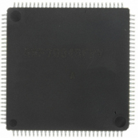
DF70845AD80FPV Renesas Electronics America, DF70845AD80FPV Datasheet - Page 44

DF70845AD80FPV
Manufacturer Part Number
DF70845AD80FPV
Description
IC SUPERH MCU FLASH 112LQFP
Manufacturer
Renesas Electronics America
Series
SuperH® SH7080r
Datasheet
1.DF70844AD80FPV.pdf
(1644 pages)
Specifications of DF70845AD80FPV
Core Size
32-Bit
Program Memory Size
512KB (512K x 8)
Core Processor
SH-2
Speed
80MHz
Connectivity
EBI/EMI, FIFO, I²C, SCI, SSU
Peripherals
DMA, POR, PWM, WDT
Number Of I /o
76
Program Memory Type
FLASH
Ram Size
32K x 8
Voltage - Supply (vcc/vdd)
3 V ~ 5.5 V
Data Converters
A/D 8x10b
Oscillator Type
Internal
Operating Temperature
-40°C ~ 85°C
Package / Case
112-LQFP
No. Of I/o's
76
Ram Memory Size
32KB
Cpu Speed
80MHz
Digital Ic Case Style
LQFP
Supply Voltage Range
3V To 3.6V, 4.5V To 5.5V
Embedded Interface Type
I2C, SCI
Rohs Compliant
Yes
Lead Free Status / RoHS Status
Lead free / RoHS Compliant
For Use With
R0K570865S001BE - KIT STARTER FOR SH7086R0K570865S000BE - KIT STARTER FOR SH7086HS0005KCU11H - EMULATOR E10A-USB H8S(X),SH2(A)
Eeprom Size
-
Lead Free Status / RoHS Status
Lead free / RoHS Compliant, Lead free / RoHS Compliant
Available stocks
Company
Part Number
Manufacturer
Quantity
Price
Company:
Part Number:
DF70845AD80FPV
Manufacturer:
TAIYO
Quantity:
40 000
Company:
Part Number:
DF70845AD80FPV
Manufacturer:
Renesas Electronics America
Quantity:
10 000
- Current page: 44 of 1644
- Download datasheet (10Mb)
Figure 28.32 Synchronous DRAM Burst Read Bus Cycle (Four Read Cycles)
Figure 28.33 Synchronous DRAM Burst Read Bus Cycle (Four Read Cycles)
Figure 28.34 Synchronous DRAM Burst Read Bus Cycle (Four Read Cycles)
Figure 28.35 Synchronous DRAM Burst Write Bus Cycle (Four Write Cycles)
Figure 28.36 Synchronous DRAM Burst Write Bus Cycle (Four Write Cycles)
Figure 28.37 Synchronous DRAM Burst Write Bus Cycle (Four Write Cycles)
Figure 28.38 Synchronous DRAM Auto-Refreshing Timing
Figure 28.39 Synchronous DRAM Self-Refreshing Timing
Figure 28.40 Synchronous DRAM Mode Register Write Timing (WTRP = 1 Cycle)............. 1450
Figure 28.41 PCMCIA Memory Card Interface Bus Timing ................................................... 1451
Figure 28.42 PCMCIA Memory Card Interface Bus Timing
Figure 28.43 PCMCIA I/O Card Interface Bus Timing............................................................ 1453
Figure 28.44 PCMCIA I/O Card Interface Bus Timing
Figure 28.45 DREQ Input Timing............................................................................................ 1455
Figure 28.46 MTU2 Input/Output Timing................................................................................ 1456
Figure 28.47 MTU2 Clock Input Timing ................................................................................. 1457
Figure 28.48 MTU2S Input/Output Timing ............................................................................. 1458
Figure 28.49 I/O Port Input/Output Timing.............................................................................. 1459
Figure 28.50 WDT Timing ....................................................................................................... 1460
Figure 28.51 Input Clock Timing ............................................................................................. 1461
Figure 28.52 SCI Input/Output Timing .................................................................................... 1462
Figure 28.53 Input Clock Timing ............................................................................................. 1463
Figure 28.54 SCIF Input/Output Timing .................................................................................. 1464
Figure 28.55 SSU Timing (Master, CPHS = 1) ........................................................................ 1466
Rev. 3.00 May 17, 2007 Page xliv of Iviii
(Bank Active Mode: ACT + READ Commands, CAS Latency 2,
WTRCD = 0 Cycle) ............................................................................................ 1442
(Bank Active Mode: READ Command, Same Row Address, CAS Latency 2,
WTRCD = 0 Cycle)
(Bank Active Mode: PRE + ACT + READ Commands,
Different Row Addresses, CAS Latency 2, WTRCD = 0 Cycle)....................... 1444
(Bank Active Mode: ACT + WRITE Commands, WTRCD = 0 Cycle,
TRWL = 0 Cycle)................................................................................................ 1445
(Bank Active Mode: WRITE Command, Same Row Address,
WTRCD = 0 Cycle, TRWL = 0 Cycle).............................................................. 1446
(Bank Active Mode: PRE + ACT + WRITE Commands,
Different Row Addresses, WTRCD = 0 Cycle, TRWL = 0 Cycle).................... 1447
(WTRP = 1 Cycle, WTRC = 3 Cycles) ............................................................... 1448
(WTRP = 1 Cycle, WTRC = 3 Cycles) ............................................................... 1449
(TED = 2.5 Cycles, TEH = 1.5 Cycles, One External Wait Cycle)..................... 1452
(TED = 2.5 Cycles, TEH = 1.5 Cycles, One External Wait Cycle)..................... 1454
.............................................................................................. 1443
Related parts for DF70845AD80FPV
Image
Part Number
Description
Manufacturer
Datasheet
Request
R

Part Number:
Description:
KIT STARTER FOR M16C/29
Manufacturer:
Renesas Electronics America
Datasheet:

Part Number:
Description:
KIT STARTER FOR R8C/2D
Manufacturer:
Renesas Electronics America
Datasheet:

Part Number:
Description:
R0K33062P STARTER KIT
Manufacturer:
Renesas Electronics America
Datasheet:

Part Number:
Description:
KIT STARTER FOR R8C/23 E8A
Manufacturer:
Renesas Electronics America
Datasheet:

Part Number:
Description:
KIT STARTER FOR R8C/25
Manufacturer:
Renesas Electronics America
Datasheet:

Part Number:
Description:
KIT STARTER H8S2456 SHARPE DSPLY
Manufacturer:
Renesas Electronics America
Datasheet:

Part Number:
Description:
KIT STARTER FOR R8C38C
Manufacturer:
Renesas Electronics America
Datasheet:

Part Number:
Description:
KIT STARTER FOR R8C35C
Manufacturer:
Renesas Electronics America
Datasheet:

Part Number:
Description:
KIT STARTER FOR R8CL3AC+LCD APPS
Manufacturer:
Renesas Electronics America
Datasheet:

Part Number:
Description:
KIT STARTER FOR RX610
Manufacturer:
Renesas Electronics America
Datasheet:

Part Number:
Description:
KIT STARTER FOR R32C/118
Manufacturer:
Renesas Electronics America
Datasheet:

Part Number:
Description:
KIT DEV RSK-R8C/26-29
Manufacturer:
Renesas Electronics America
Datasheet:

Part Number:
Description:
KIT STARTER FOR SH7124
Manufacturer:
Renesas Electronics America
Datasheet:

Part Number:
Description:
KIT STARTER FOR H8SX/1622
Manufacturer:
Renesas Electronics America
Datasheet:

Part Number:
Description:
KIT DEV FOR SH7203
Manufacturer:
Renesas Electronics America
Datasheet:


