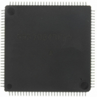
DF70845AD80FPV Renesas Electronics America, DF70845AD80FPV Datasheet - Page 993

DF70845AD80FPV
Manufacturer Part Number
DF70845AD80FPV
Description
IC SUPERH MCU FLASH 112LQFP
Manufacturer
Renesas Electronics America
Series
SuperH® SH7080r
Datasheet
1.DF70844AD80FPV.pdf
(1644 pages)
Specifications of DF70845AD80FPV
Core Size
32-Bit
Program Memory Size
512KB (512K x 8)
Core Processor
SH-2
Speed
80MHz
Connectivity
EBI/EMI, FIFO, I²C, SCI, SSU
Peripherals
DMA, POR, PWM, WDT
Number Of I /o
76
Program Memory Type
FLASH
Ram Size
32K x 8
Voltage - Supply (vcc/vdd)
3 V ~ 5.5 V
Data Converters
A/D 8x10b
Oscillator Type
Internal
Operating Temperature
-40°C ~ 85°C
Package / Case
112-LQFP
No. Of I/o's
76
Ram Memory Size
32KB
Cpu Speed
80MHz
Digital Ic Case Style
LQFP
Supply Voltage Range
3V To 3.6V, 4.5V To 5.5V
Embedded Interface Type
I2C, SCI
Rohs Compliant
Yes
Lead Free Status / RoHS Status
Lead free / RoHS Compliant
For Use With
R0K570865S001BE - KIT STARTER FOR SH7086R0K570865S000BE - KIT STARTER FOR SH7086HS0005KCU11H - EMULATOR E10A-USB H8S(X),SH2(A)
Eeprom Size
-
Lead Free Status / RoHS Status
Lead free / RoHS Compliant, Lead free / RoHS Compliant
Available stocks
Company
Part Number
Manufacturer
Quantity
Price
Company:
Part Number:
DF70845AD80FPV
Manufacturer:
TAIYO
Quantity:
40 000
Company:
Part Number:
DF70845AD80FPV
Manufacturer:
Renesas Electronics America
Quantity:
10 000
- Current page: 993 of 1644
- Download datasheet (10Mb)
18.4.8
Flowcharts in respective modes that use the I
18.21.
Example of Use
Figure 18.18 Sample Flowchart for Master Transmit Mode
No
No
No
Write transmit data in ICDRT
Write transmit data in ICDRT
No
No
No
Set MST to 1 and TRS
Read ACKBR in ICIER
Read BBSY in ICCR2
Read TDRE in ICSR
Read TEND in ICSR
Clear TEND in ICSR
Clear STOP in ICSR
Read STOP in ICSR
Clear TDRE in ICSR
Read TEND in ICSR
Write transmit data
Set MST and TRS
Write 1 to BBSY
Write 0 to BBSY
to 0 in ICCR1
in ICCR1 to 1
and 0 to SCP
ACKBR=0 ?
TEND=1 ?
TDRE=1 ?
TEND=1 ?
STOP=1 ?
BBSY=0 ?
Last byte?
in ICDRT
Transmit
Initialize
and SCP
mode?
Start
End
Yes
Yes
Yes
Yes
Yes
Yes
Yes
Yes
No
No
[1]
[2]
[3]
[4]
[5]
[6]
[7]
[8]
[9]
[10]
[11]
[12]
[13]
[14]
[15]
Mater receive mode
[1]
[2]
[3]
[4]
[5]
[6]
[7]
[8]
[9]
[10] Wait for last byte to be transmitted.
[11] Clear the TEND flag.
[12] Clear the STOP flag.
[13] Issue the stop condition.
[14] Wait for the creation of stop condition.
[15] Set slave receive mode. Clear TDRE.
Test the status of the SCL and SDA lines.
Set master transmit mode.
Issue the start condition.
Set the first byte (slave address + R/W) of transmit data.
Wait for 1 byte to be transmitted.
Test the acknowledge transferred from the specified slave device.
Set the second and subsequent bytes (except for the final byte) of transmit data.
Wait for ICDRT empty.
Set the last byte of transmit data.
2
C bus interface 2 are shown in figures 18.18 to
Rev. 3.00 May 17, 2007 Page 935 of 1582
Section 18 I
2
C Bus Interface 2 (I
REJ09B0181-0300
2
C2)
Related parts for DF70845AD80FPV
Image
Part Number
Description
Manufacturer
Datasheet
Request
R

Part Number:
Description:
KIT STARTER FOR M16C/29
Manufacturer:
Renesas Electronics America
Datasheet:

Part Number:
Description:
KIT STARTER FOR R8C/2D
Manufacturer:
Renesas Electronics America
Datasheet:

Part Number:
Description:
R0K33062P STARTER KIT
Manufacturer:
Renesas Electronics America
Datasheet:

Part Number:
Description:
KIT STARTER FOR R8C/23 E8A
Manufacturer:
Renesas Electronics America
Datasheet:

Part Number:
Description:
KIT STARTER FOR R8C/25
Manufacturer:
Renesas Electronics America
Datasheet:

Part Number:
Description:
KIT STARTER H8S2456 SHARPE DSPLY
Manufacturer:
Renesas Electronics America
Datasheet:

Part Number:
Description:
KIT STARTER FOR R8C38C
Manufacturer:
Renesas Electronics America
Datasheet:

Part Number:
Description:
KIT STARTER FOR R8C35C
Manufacturer:
Renesas Electronics America
Datasheet:

Part Number:
Description:
KIT STARTER FOR R8CL3AC+LCD APPS
Manufacturer:
Renesas Electronics America
Datasheet:

Part Number:
Description:
KIT STARTER FOR RX610
Manufacturer:
Renesas Electronics America
Datasheet:

Part Number:
Description:
KIT STARTER FOR R32C/118
Manufacturer:
Renesas Electronics America
Datasheet:

Part Number:
Description:
KIT DEV RSK-R8C/26-29
Manufacturer:
Renesas Electronics America
Datasheet:

Part Number:
Description:
KIT STARTER FOR SH7124
Manufacturer:
Renesas Electronics America
Datasheet:

Part Number:
Description:
KIT STARTER FOR H8SX/1622
Manufacturer:
Renesas Electronics America
Datasheet:

Part Number:
Description:
KIT DEV FOR SH7203
Manufacturer:
Renesas Electronics America
Datasheet:


