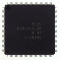
M30845FJGP#U3 Renesas Electronics America, M30845FJGP#U3 Datasheet - Page 209

M30845FJGP#U3
Manufacturer Part Number
M30845FJGP#U3
Description
IC M32C MCU FLASH 512K 144LQFP
Manufacturer
Renesas Electronics America
Series
M16C™ M32C/80r
Specifications of M30845FJGP#U3
Core Processor
M32C/80
Core Size
16/32-Bit
Speed
32MHz
Connectivity
CAN, I²C, IEBus, SIO, UART/USART
Peripherals
DMA, PWM, WDT
Number Of I /o
121
Program Memory Size
512KB (512K x 8)
Program Memory Type
FLASH
Ram Size
24K x 8
Voltage - Supply (vcc/vdd)
3 V ~ 5.5 V
Data Converters
A/D 34x10b, D/A 2x8b
Oscillator Type
Internal
Operating Temperature
-40°C ~ 85°C
Package / Case
144-LQFP
Lead Free Status / RoHS Status
Lead free / RoHS Compliant
Eeprom Size
-
Available stocks
Company
Part Number
Manufacturer
Quantity
Price
- Current page: 209 of 531
- Download datasheet (4Mb)
R
R
M
e
E
3
. v
J
Figure 16.3 INVC1 Register
2
0
C
1
9
0 .
B
8 /
0
1
4
0
3
J
G
6
u
Three-Phase PWM Control Register 1
o r
b7
0
0 -
. l
NOTES:
TA11, TA21 and TA41 Registers Not used
INV01 and INV00 Bit
in the INVC0 Register
INV13 Bit
Mode
0
1
u
b6
, 7
0
p
1. Rewrite the INVC1 register after the PRC1 bit in the PRCR register is set to "1" (write enable).
2. The following table lists how the INV11 bit setting works.
3. When the INV06 bit in the INVC0 registser is set to "1" (sawtooth wave modulation mode), set the
4. The INV13 bit setting is enabled only when the INV06 bit is set to "0" (Triangular wave modulation
5. If the following conditions are all met, set the INV16 bit to "1".
1
(
The timers A1, A2, A4, and B2 must be stopped during rewrite.
2
INV11 bit to "0". Also, when the INV11 bit is set to "0", set the PWCON bit in the TB2SC register to
"0" (Timer B2 counter underflows).
mode) and the INV11 bit to "1".
If the above conditions are not met, set the INV16 bit to "0".
b5
M
0
0
3
• The INV15 bit is set to "0"
• The Dij bit (i=U, V or W, j=0, 1) and DiBj bit always have different values when the INV03 bit in
b4
5
Item
2
the INVC0 register is set to "1". (The positive-phase and negative-phase outputs always provide
opposite level signals.)
C
b3
8 /
Page 186
, 4
b2
M
b1
3
2
b0
C
f o
8 /
INV16
Symbol
INV10
INV11
INV12
INV13
INV14
INV15
Three-phase mode 0
4
Disabled. The ICTB2 counter is
incremented whenever the timer B2
counter underflows
Disabled
4
(b7)
9
) T
Bit
Symbol
INVC1
5
Carrier Wave Detect Flag
Timer A1, A2 and A4
Start Trigger Select Bit
Timer A1-1, A2-1 and
A4-1 Control Bit
Dead Time Timer
Count Source Select Bit
Output Polarity Control Bit
Dead Time Disable Bit
Dead Time Timer Trigger
Select Bit
Reserved Bit
INV11 = 0
Bit Name
Address
0309
(2, 3)
16
(1)
(4)
16. Three-Phase Motor Control Timer Functions
0: Timer B2 counter underflows
1: Timer B2 counter underflows and
0: Three-phase mode 0
1: Three-phase mode 1
0 : f
1 : f
0: Timer A1 reload control signal is "0"
1: Timer A1 reload control signal is "1"
0 : Active "L" of an output waveform
1 : Active "H" of an output waveform
0: Enables dead time
1: Disables dead time
0: Falling edge of a one-shot pulse of
1: Rising edge of the three-phase output
Set to "0"
the timer A1, A2 and A4
write to the TB2 register
shift register (U-, V-, W-phase)
Three-phase mode 1
Used
Enabled
1
1
Enabled when INV11=1 and INV06=0
divided-by-2
After Reset
00
16
Function
INV11 = 1
(5)
RW
RW
RW
RW
RW
RW
RW
RW
RO
Related parts for M30845FJGP#U3
Image
Part Number
Description
Manufacturer
Datasheet
Request
R

Part Number:
Description:
KIT STARTER FOR M16C/29
Manufacturer:
Renesas Electronics America
Datasheet:

Part Number:
Description:
KIT STARTER FOR R8C/2D
Manufacturer:
Renesas Electronics America
Datasheet:

Part Number:
Description:
R0K33062P STARTER KIT
Manufacturer:
Renesas Electronics America
Datasheet:

Part Number:
Description:
KIT STARTER FOR R8C/23 E8A
Manufacturer:
Renesas Electronics America
Datasheet:

Part Number:
Description:
KIT STARTER FOR R8C/25
Manufacturer:
Renesas Electronics America
Datasheet:

Part Number:
Description:
KIT STARTER H8S2456 SHARPE DSPLY
Manufacturer:
Renesas Electronics America
Datasheet:

Part Number:
Description:
KIT STARTER FOR R8C38C
Manufacturer:
Renesas Electronics America
Datasheet:

Part Number:
Description:
KIT STARTER FOR R8C35C
Manufacturer:
Renesas Electronics America
Datasheet:

Part Number:
Description:
KIT STARTER FOR R8CL3AC+LCD APPS
Manufacturer:
Renesas Electronics America
Datasheet:

Part Number:
Description:
KIT STARTER FOR RX610
Manufacturer:
Renesas Electronics America
Datasheet:

Part Number:
Description:
KIT STARTER FOR R32C/118
Manufacturer:
Renesas Electronics America
Datasheet:

Part Number:
Description:
KIT DEV RSK-R8C/26-29
Manufacturer:
Renesas Electronics America
Datasheet:

Part Number:
Description:
KIT STARTER FOR SH7124
Manufacturer:
Renesas Electronics America
Datasheet:

Part Number:
Description:
KIT STARTER FOR H8SX/1622
Manufacturer:
Renesas Electronics America
Datasheet:

Part Number:
Description:
KIT DEV FOR SH7203
Manufacturer:
Renesas Electronics America
Datasheet:


